
Product ID: UCMIG15H2036
Report ID:
UCMIG15H2036 |
Region:
Global |
Published Date: Upcoming |
Pages:
165
| Tables: 55 | Figures: 60
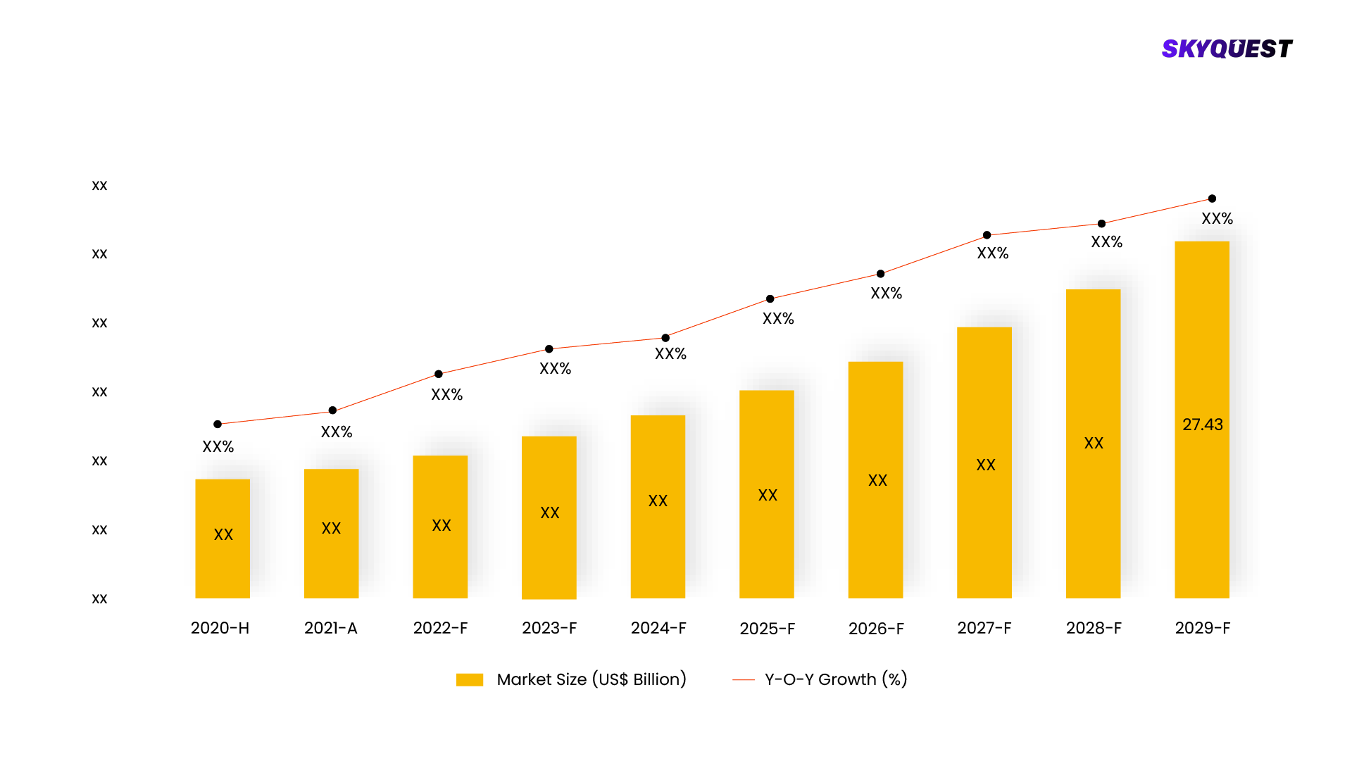
The market size of Fan-Out Wafer Level Packaging reached over USD 2.5 billion in 2022 and is projected to experience a compound annual growth rate (CAGR) exceeding 10% from 2023 to 2032. The global fan-out wafer level packaging industry is being propelled by an increasing demand for advanced and cost-efficient packaging technologies, coupled with the ongoing trends of digitalization and miniaturization. The evolving technological landscape necessitates the continual reduction in the size and enhancement of portability of electronic devices. Utilizing the fan-out wafer level packaging technology enables the consolidation of multiple components onto a single substrate, resulting in more compact and energy-efficient modules.
This report is being written to illustrate the market opportunity by region and by segments, indicating opportunity areas for the vendors to tap upon. To estimate the opportunity, it was very important to understand the current market scenario and the way it will grow in future.
Production and consumption patterns are being carefully compared to forecast the market. Other factors considered to forecast the market are the growth of the adjacent market, revenue growth of the key market vendors, scenario-based analysis, and market segment growth.
The market size was determined by estimating the market through a top-down and bottom-up approach, which was further validated with industry interviews. Considering the nature of the market we derived the Paper Packaging by segment aggregation, the contribution of the Paper Packaging in Diversified Materials and vendor share.
To determine the growth of the market factors such as drivers, trends, restraints, and opportunities were identified, and the impact of these factors was analyzed to determine the market growth. To understand the market growth in detail, we have analyzed the year-on-year growth of the market. Also, historic growth rates were compared to determine growth patterns.
Our industry expert will work with you to provide you with customized data in a short amount of time.
REQUEST FREE CUSTOMIZATIONWant to customize this report? This report can be personalized according to your needs. Our analysts and industry experts will work directly with you to understand your requirements and provide you with customized data in a short amount of time. We offer $1000 worth of FREE customization at the time of purchase.
Product ID: UCMIG15H2036
 USA (+1) 351-333-4748
