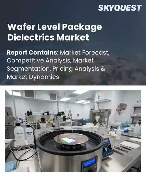
Wafer Level Package Dielectrics Market
Report ID: SQMIG15E4306
Report ID: SQMIG15E4306
[email protected]
USA +1 351-333-4748
Report ID:
SQMIG15E4306 |
Region:
Global |
Published Date: September, 2026
Pages:
157
|Tables:
124
|Figures:
77


Global Wafer Level Package Dielectrics Market size was valued at USD 1.85 Billion in 2024 and is poised to grow from USD 1.98 Billion in 2025 to USD 3.37 Billion by 2033, growing at a CAGR of 6.9% during the forecast period (2026-2033).
The wafer‑level package (WLP) dielectrics market encompasses insulating materials applied directly onto silicon wafers to enable interconnects, protect circuitry, and support signal integrity in semiconductor devices. Its significance stems from the push toward miniaturization, where package‑on‑package approaches cannot meet the thermal demands of 5‑nm and smaller nodes. Historically, the market emerged in the early 2010s as partners adopted low‑k polymers and silicon‑based oxides to replace bulk silicon, exemplified by TSMC’s integration of epoxy‑based dielectrics for its 7‑nm chiplets. This evolution has accelerated as device architects seek to reduce parasitic capacitance, establishing dielectrics as a cornerstone, critical long‑term future for packaging. Among the catalysts driving expansion of the wafer‑level package dielectrics market, the surge in heterogeneous integration stands out because it forces designers to stack diverse chips within a footprint, demanding dielectric layers that preserve signal speed while preventing thermal runaway. Adoption of 3‑D‑ICs in automotive radar modules illustrates this dynamic; manufacturers combine silicon sensors with drivers, so the dielectric stack must isolate pathways without adding bulk, prompting suppliers to develop fluorinated polymers with dielectric constants below 2.0. These innovations open revenue streams in data‑center accelerators and wearables, where reduced latency and size constraints translate into advantage, thereby amplifying market upside.
How is AI-driven automation impacting the wafer-level package dielectrics market?
AI driven automation is reshaping the wafer level package dielectrics market by embedding machine learning into material formulation, deposition and inspection steps. Algorithms analyze sensor data in real time to adjust plasma parameters, temperature and flow rates, which reduces defect density and improves uniformity across large wafers. Designers use predictive models to select dielectric chemistries that meet electrical performance while minimizing material waste. Production lines benefit from autonomous defect detection that triggers immediate corrective actions, shortening cycle time and raising overall yield. The result is a more agile supply chain that can respond quickly to the demand for higher density interconnects in advanced semiconductor devicesIn June 2024, a leading wafer level packaging firm announced the integration of AI driven automation into its dielectric deposition line, boosting throughput and consistency while lowering energy use. The system learns from each run, refining process windows and reducing scrap, which accelerates time to market for high performance chips.
Market snapshot - (2026-2033)
Global Market Size
USD 1.85 Billion
Largest Segment
Polyimide
Fastest Growth
Polybenzoxazole
Growth Rate
6.9% CAGR
To get more insights on this market click here to Request a Free Sample Report
Global wafer level package dielectrics market is segmented by material chemistry, packaging type, application, end use industry and region. Based on material chemistry, the market is segmented into Polyimide, Polybenzoxazole, Benzocyclobutene, Epoxy Resins and Others. Based on packaging type, the market is segmented into Fan In WLP, Fan Out WLP, Flip Chip Packaging and 2.5D 3D IC Stacking. Based on application, the market is segmented into Power Amplifiers, Baseband Processors, Image Sensors, RF Filters, Power Management ICs and Others. Based on end use industry, the market is segmented into Consumer Electronics, Automotive Electronics, Telecommunications IT and Aerospace Defense. Based on region, the market is segmented into North America, Europe, Asia Pacific, Latin America and Middle East & Africa.
Polyimide segment dominates because its exceptional thermal stability and mechanical flexibility meet the rigorous reliability demands of advanced wafer level package dielectric layers. Designers favor polyimide for its ability to endure high temperature processing while maintaining a low dielectric constant, which supports signal integrity in dense interconnects. The material’s proven track record in high performance applications and compatibility with existing fab equipment reinforce its leading position in the market.
However, benzocyclobutene is witnessing the strongest growth momentum because its low moisture absorption and excellent planarization characteristics enable ultra fine pitch interconnects in emerging high frequency modules. The rising adoption of 5G front end modules and substrate level integration drives demand, positioning it as a catalyst for future market expansion.
Fan Out WLP segment leads because its ability to spread die area beyond the chip footprint accommodates a higher I/O count while maintaining thin profile, satisfying the demand for compact high performance modules. The architecture reduces package parasitics and supports advanced signal routing, making it the preferred choice for next generation smartphones and high bandwidth communication devices, thus cementing its leadership in wafer level package dielectrics.
Meanwhile, Fan In WLP is emerging as the key high growth area because its simpler process flow and lower cost enable rapid scaling for mass market products. The surge in wearables and IoT sensors, which need modest I/O density but high volume production, fuels its expansion and creates opportunities for dielectric innovation within this packaging style.
To get detailed segments analysis, Request a Free Sample Report
The region benefits from a tightly integrated semiconductor ecosystem where leading foundries, advanced packaging specialists, and material suppliers coexist in close proximity. Robust R&D networks supported by collaborative industry clusters accelerate innovation in low‑k and high‑performance dielectric formulations. Strong governmental incentives encourage technology adoption and capital investment, fostering a rapid turnover of next‑generation devices. A mature supply chain ensures reliable sourcing of high‑purity chemicals and precision manufacturing equipment, reducing lead times and enhancing product consistency. Moreover, the concentration of consumer electronics manufacturers drives sustained demand for high‑density interconnects, positioning Asia Pacific as the pivotal hub for wafer level package dielectric advancement.
Wafer Level Package Dielectrics Market in Japan is propelled by a legacy of precision engineering and a dense network of semiconductor fabs that prioritize advanced packaging solutions. Collaborative research institutions provide continuous breakthroughs in material performance, while domestic equipment manufacturers ensure seamless integration of novel dielectric processes. The market also benefits from strong alignment with automotive electronics and high‑end consumer devices, reinforcing demand for reliable, high‑frequency dielectric layers.
Wafer Level Package Dielectrics Market in South Korea thrives on the presence of world‑leading memory and logic foundries that demand cutting‑edge dielectric technologies. A vibrant start‑up culture focused on material science complements extensive corporate R&D programs, driving rapid adoption of low‑loss and high‑reliability dielectric solutions. Close coordination between chip designers and packaging houses accelerates product development cycles, reinforcing the country’s role as a key driver of regional market leadership.
North America’s growth is fueled by a strong emphasis on innovation within high‑performance computing, aerospace, and defense sectors that require sophisticated packaging solutions. Leading research universities and private labs propel material science advances, while a flexible investment environment supports scaling of pilot lines into full‑scale production. Close collaboration between chip designers and contract manufacturers accelerates time‑to‑market for novel dielectric formulations. Policy frameworks that promote advanced manufacturing and secure supply chains further enhance confidence among equipment suppliers and end‑users, creating a fertile landscape for continued expansion.
Wafer Level Package Dielectrics Market in the United States is anchored by expansive semiconductor design hubs that drive early adoption of high‑frequency dielectric materials. Strong venture capital flows enable start‑ups specializing in nanostructured dielectrics to scale rapidly. Integration of advanced testing facilities ensures rigorous qualification, while close ties with defense contractors reinforce demand for robust, low‑loss dielectric layers across mission‑critical applications.
Wafer Level Package Dielectrics Market in Canada benefits from a collaborative ecosystem linking research institutions with a growing number of specialty material firms. Emphasis on sustainable manufacturing practices encourages the development of eco‑friendly dielectric formulations. Proximity to major automotive and communications manufacturers supports steady demand for reliable packaging solutions that meet stringent performance criteria.
Europe leverages its deep expertise in precision engineering and environmental standards to advance wafer level package dielectric technologies. A network of multinational research consortia fosters cross‑border collaboration, accelerating the translation of laboratory breakthroughs into industrial applications. The region’s focus on circular economy principles drives the pursuit of recyclable and low‑impact dielectric materials. Robust regulatory frameworks encourage high reliability and safety, appealing to aerospace, automotive, and medical device manufacturers. Strategic public‑private partnerships also fund scale‑up initiatives, reinforcing Europe’s emerging leadership in the sector.
Wafer Level Package Dielectrics Market in Germany is shaped by a strong automotive electronics sector that demands high‑reliability dielectric layers for power management and sensor integration. Close cooperation between equipment manufacturers and material suppliers ensures seamless process integration, while research institutes provide continuous innovation in dielectric chemistry and nanostructuring.
Wafer Level Package Dielectrics Market in the United Kingdom is driven by a vibrant fintech and telecommunications landscape that requires high‑speed, low‑loss dielectric solutions. Collaborative hubs linking universities with niche material firms accelerate development of customized dielectric formulations tailored to emerging connectivity standards.
Wafer Level Package Dielectrics Market in France benefits from a strong aerospace and defense base that prioritizes lightweight, high‑performance packaging. Close ties between research laboratories and industrial partners foster rapid prototyping of advanced dielectric materials, supporting the nation’s push for higher integration densities.
To know more about the market opportunities by region and country, click here to
Buy The Complete Report
Advanced Chip Miniaturization Demands
Emerging 5G and AI Applications
High Cost of Material Development
Complex Integration Process Challenges
Request Free Customization of this report to help us to meet your business objectives.
Top Player’s Company Profile
Recent Developments
SkyQuest’s ABIRAW (Advanced Business Intelligence, Research & Analysis Wing) is our Business Information Services team that Collects, Collates, Correlates, and Analyses the Data collected by means of Primary Exploratory Research backed by robust Secondary Desk research. As per SkyQuest analysis, the market is propelled primarily by advanced chip miniaturization demands, which push manufacturers toward low‑k dielectrics that enable finer interconnects and reliable thermal management. A second catalyst is the rapid expansion of 5G and AI applications that require high‑frequency, low‑loss materials for dense, high‑performance packages. The polyimide chemistry segment remains the clear leader because of its thermal stability and flexibility, while fan‑out WLP drives the highest material usage in advanced packaging. Asia Pacific dominates globally thanks to its integrated semiconductor ecosystem and strong consumer electronics demand. However, the high cost of material development acts as a significant restraint, slowing wider adoption.
| Report Metric | Details |
|---|---|
| Market size value in 2024 | USD 1.85 Billion |
| Market size value in 2033 | USD 3.37 Billion |
| Growth Rate | 6.9% |
| Base year | 2024 |
| Forecast period | (2026-2033) |
| Forecast Unit (Value) | USD Billion |
| Segments covered |
|
| Regions covered | North America (US, Canada), Europe (Germany, France, United Kingdom, Italy, Spain, Rest of Europe), Asia Pacific (China, India, Japan, Rest of Asia-Pacific), Latin America (Brazil, Rest of Latin America), Middle East & Africa (South Africa, GCC Countries, Rest of MEA) |
| Companies covered |
|
| Customization scope | Free report customization with purchase. Customization includes:-
|
To get a free trial access to our platform which is a one stop solution for all your data requirements for quicker decision making. This platform allows you to compare markets, competitors who are prominent in the market, and mega trends that are influencing the dynamics in the market. Also, get access to detailed SkyQuest exclusive matrix.
Table Of Content
Executive Summary
Market overview
Parent Market Analysis
Market overview
Market size
KEY MARKET INSIGHTS
COVID IMPACT
MARKET DYNAMICS & OUTLOOK
Market Size by Region
KEY COMPANY PROFILES
Methodology
For the Wafer Level Package Dielectrics Market, our research methodology involved a mixture of primary and secondary data sources. Key steps involved in the research process are listed below:
1. Information Procurement: This stage involved the procurement of Market data or related information via primary and secondary sources. The various secondary sources used included various company websites, annual reports, trade databases, and paid databases such as Hoover's, Bloomberg Business, Factiva, and Avention. Our team did 45 primary interactions Globally which included several stakeholders such as manufacturers, customers, key opinion leaders, etc. Overall, information procurement was one of the most extensive stages in our research process.
2. Information Analysis: This step involved triangulation of data through bottom-up and top-down approaches to estimate and validate the total size and future estimate of the Wafer Level Package Dielectrics Market.
3. Report Formulation: The final step entailed the placement of data points in appropriate Market spaces in an attempt to deduce viable conclusions.
4. Validation & Publishing: Validation is the most important step in the process. Validation & re-validation via an intricately designed process helped us finalize data points to be used for final calculations. The final Market estimates and forecasts were then aligned and sent to our panel of industry experts for validation of data. Once the validation was done the report was sent to our Quality Assurance team to ensure adherence to style guides, consistency & design.
Analyst Support
Customization Options
With the given market data, our dedicated team of analysts can offer you the following customization options are available for the Wafer Level Package Dielectrics Market:
Product Analysis: Product matrix, which offers a detailed comparison of the product portfolio of companies.
Regional Analysis: Further analysis of the Wafer Level Package Dielectrics Market for additional countries.
Competitive Analysis: Detailed analysis and profiling of additional Market players & comparative analysis of competitive products.
Go to Market Strategy: Find the high-growth channels to invest your marketing efforts and increase your customer base.
Innovation Mapping: Identify racial solutions and innovation, connected to deep ecosystems of innovators, start-ups, academics, and strategic partners.
Category Intelligence: Customized intelligence that is relevant to their supply Markets will enable them to make smarter sourcing decisions and improve their category management.
Public Company Transcript Analysis: To improve the investment performance by generating new alpha and making better-informed decisions.
Social Media Listening: To analyze the conversations and trends happening not just around your brand, but around your industry as a whole, and use those insights to make better Marketing decisions.
REQUEST FOR SAMPLE
 REQUEST FREE CUSTOMIZATION


Want to customize this report? This report can be personalized according to your needs. Our analysts and industry experts will work directly with you to understand your requirements and provide you with customized data in a short amount of time. We offer $1000 worth of FREE customization at the time of purchase.
Feedback From Our Clients


 USA (+1) 351-333-4748

