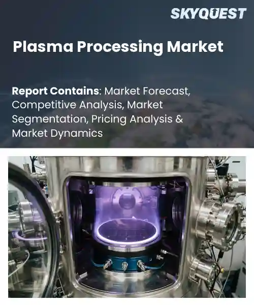
Plasma Processing Market
Report ID: SQMIG45N2289
Report ID: SQMIG45N2289
[email protected]
USA +1 351-333-4748
Report ID:
SQMIG45N2289 |
Region:
Global |
Published Date: November, 2026
Pages:
157
|Tables:
124
|Figures:
77


Global Plasma Processing Market size was valued at USD 7.2 Billion in 2024 and is poised to grow from USD 7.76 Billion in 2025 to USD 14.16 Billion by 2033, growing at a CAGR of 7.8% during the forecast period (2026-2033).
The global plasma processing market comprises technologies that use ionized gases to modify surfaces, etch microstructures, or deposit thin films across industries such as semiconductors, aerospace, and medical devices. Its importance stems from the ability to achieve nanometer‑scale precision while reducing chemical waste, a combination that drives cost efficiency and sustainability in manufacturing. Historically, plasma etching emerged in the 1970s for integrated‑circuit fabrication and expanded in the 1990s to thin‑film deposition for display panels. Recent advances in high‑density inductively coupled plasma sources have accelerated adoption, illustrated by semiconductor fabs transitioning from wet‑chemistry to plasma‑based patterning to meet sub‑10‑nanometer node requirements. The next pivotal factor shaping the plasma processing market is the surge in demand for advanced packaging and three‑dimensional integrated circuits, which require precise, low‑damage etching at ever‑smaller pitches. As chip designers pursue higher functionality per wafer, plasma‑based direct‑write and atomic‑layer‑deposition techniques enable layer‑by‑layer construction without compromising yield, thereby unlocking new revenue streams for fab operators. This technical capability attracts automotive and IoT manufacturers seeking robust, miniaturized sensors; for example, plasma‑engraved silicon‑on‑insulator wafers now power radar modules in autonomous vehicles. Consequently, equipment suppliers are expanding their portfolios with modular, AI‑controlled plasma reactors, translating the technology’s scalability into tangible market expansion.
How are AI and IoT integration improving productivity in the plasma processing market?
AI and IoT are converging to reshape plasma processing by turning equipment into self optimizing platforms. Sensors embedded in reactors feed continuous data on temperature, gas flow and plasma density to cloud based analytics that predict wear and suggest parameter tweaks. This predictive capability reduces unplanned shutdowns and shortens cycle times. Operators can monitor multiple tools from a single dashboard, enabling rapid response to drift and uniformity issues. The market now sees tighter integration of machine learning models with edge devices, allowing real time recipe adjustments that boost yield while conserving energy. These advances are driving higher plant efficiency and faster time to market for semiconductor manufacturers.Applied Materials June 2024, introduced an AI driven IoT enabled plasma etch system that continuously optimizes power settings and gas flows based on sensor feedback. The solution cuts cycle time and improves uniformity, demonstrating how intelligent integration accelerates productivity and supports growth in the plasma processing market.
Market snapshot - (2026-2033)
Global Market Size
USD 7.2 Billion
Largest Segment
Plasma Etching
Fastest Growth
Plasma Surface Modification
Growth Rate
7.8% CAGR
To get more insights on this market click here to Request a Free Sample Report
Global plasma processing market is segmented by process type, plasma source, application, end user and region. Based on process type, the market is segmented into Plasma Etching, Plasma Deposition, Plasma Cleaning, Plasma Surface Modification and Other Plasma Processes. Based on plasma source, the market is segmented into Inductively Coupled Plasma, Capacitively Coupled Plasma, Microwave Plasma, Atmospheric Pressure Plasma and Other Plasma Sources. Based on application, the market is segmented into Semiconductor Manufacturing, Electronics & Display Manufacturing, Medical Device Processing, Automotive & Aerospace and Other Applications. Based on end user, the market is segmented into Semiconductor Manufacturers, Electronics Manufacturers, Industrial Manufacturers and Research Institutions. Based on region, the market is segmented into North America, Europe, Asia Pacific, Latin America and Middle East & Africa.
Plasma etching segment dominates because it provides the critical precision required for nanoscale feature definition in modern electronic components. Its ability to selectively remove material with atomic‑level control enables manufacturers to meet stringent design tolerances, reducing defect rates and enhancing yield. This precision, combined with compatibility across a broad range of substrates, makes plasma etching the preferred choice for high‑volume production, sustaining its leadership in the market.
However, plasma deposition segment is witnessing the strongest growth momentum because emerging thin‑film technologies demand conformal coating solutions for advanced power electronics and flexible displays. Innovations in high‑density sources and low‑temperature processes expand applicability to new materials, driving rapid adoption and creating fresh revenue streams that are accelerating market expansion.
Inductively coupled plasma segment leads because it provides high plasma density with uniformity essential for large‑area etching and deposition. Efficient power coupling shortens cycle time, boosting throughput for high‑volume semiconductor fabs. Its scalability and mature equipment ecosystem make it the manufacturing backbone. Additionally, the ability to finely tune ion energy and ion flux supports diverse material chemistries, which strengthens its appeal across multiple product lines and sustains its market leadership.
Meanwhile, atmospheric pressure plasma segment emerges as a high‑growth area because its ability to operate without vacuum simplifies integration into line‑side processing and reduces capital expenditure. The rise of flexible electronics, printed circuit boards and surface‑functionalized medical components fuels demand for ambient‑condition treatments, prompting equipment deployment and expanding the market opportunity.
To get detailed segments analysis, Request a Free Sample Report
The region benefits from a deep integration of semiconductor and display manufacturing ecosystems that rely heavily on advanced plasma techniques. Robust research institutions and well‑funded corporate R&D programs drive continuous innovation in plasma source design and process optimization. Strong governmental support for high‑technology sectors encourages capital investment in cutting‑edge equipment, while a skilled engineering talent pool sustains rapid product development cycles. Close proximity of component suppliers, equipment manufacturers, and end‑users creates efficient supply chains that reduce lead times and enhance collaborative problem solving. These factors collectively reinforce Asia Pacific’s position as a hub for both technology leadership and large‑scale production capacity in the plasma processing arena.
Plasma Processing Market in Japan is anchored by world‑leading semiconductor fabs and a mature display panel industry that demand highly precise etching and deposition capabilities. Collaborative research between universities and equipment manufacturers fuels breakthroughs in low‑damage plasma processes, supporting next‑generation device architectures. The emphasis on sustainability also encourages adoption of plasma‑based cleaning and surface modification solutions across advanced manufacturing sectors.
Plasma Processing Market in South Korea is propelled by a dynamic electronics and automotive supply chain that leverages plasma technology for lithography, thin‑film deposition, and surface functionalization. Government‑backed innovation programs nurture expertise in plasma chemistry and equipment engineering, enabling rapid scaling of new process solutions. The nation’s focus on high‑density memory and flexible displays further amplifies demand for sophisticated plasma processing tools that deliver superior uniformity and throughput.
North America’s expansion is fueled by a strong emphasis on innovation in semiconductor scaling, advanced packaging, and emerging industries such as quantum devices and renewable energy components. A vibrant ecosystem of research universities, venture capital, and leading equipment manufacturers creates a fertile environment for the development of next‑generation plasma sources and control software. Close collaboration between device designers and equipment suppliers promotes tailored solutions that address complex patterning and material challenges. Furthermore, intense focus on environmental compliance and energy efficiency drives adoption of plasma‑based cleaning and surface treatment processes across diverse manufacturing sectors, reinforcing the region’s competitive edge.
Plasma Processing Market in the United States is driven by a concentration of leading semiconductor foundries and a prolific design community that demand cutting‑edge etch and deposition technologies. Strong ties between research institutions and industry accelerate the translation of plasma science breakthroughs into commercial equipment. The emphasis on high‑performance computing and AI chips creates a persistent need for ultra‑precise plasma processes that enable fine patterning and material integration. Additionally, a growing focus on sustainable manufacturing encourages the deployment of plasma‑based cleaning and surface modification solutions.
Plasma Processing Market in Canada benefits from a robust research landscape that emphasizes materials engineering and clean technology. Collaborative initiatives between academic labs and equipment suppliers foster development of plasma processes tailored for aerospace, medical device, and renewable energy applications. The nation’s commitment to environmental stewardship promotes the use of plasma techniques for waste reduction and surface treatment, positioning Canada as a growing hub for innovative plasma solutions within North America.
Europe leverages its reputation for precision engineering, stringent quality standards, and collaborative research frameworks to enhance its role in plasma processing. Integrated projects across multiple nations foster shared expertise in plasma chemistry, advanced diagnostics, and equipment reliability, supporting sectors such as microelectronics, automotive, and sustainable manufacturing. Strong policy focus on circular economy and energy efficiency drives the adoption of plasma‑based surface treatment and cleaning technologies that reduce waste and lower emissions. Moreover, a dense network of specialized suppliers and a skilled workforce enables rapid iteration of process solutions, reinforcing Europe’s standing as a center of high‑value, technology‑driven plasma applications.
Plasma Processing Market in Germany is closely tied to its world‑renowned automotive and precision manufacturing sectors, which demand high‑accuracy plasma etching and coating processes. Collaborative research consortia bring together universities, research institutes, and equipment firms to push the boundaries of plasma diagnostics and process control. The focus on energy‑efficient production and stringent environmental regulations further motivates the integration of plasma‑based cleaning and surface functionalization across industrial operations.
Plasma Processing Market in the United Kingdom draws strength from a vibrant academic environment and a growing semiconductor design community that require sophisticated plasma tools for advanced device fabrication. Public‑private partnerships support the development of low‑damage plasma processes suitable for emerging technologies such as flexible electronics and photonics. Emphasis on sustainability encourages the adoption of plasma techniques for waste minimization and surface modification in diverse manufacturing domains.
Plasma Processing Market in France is propelled by a strong emphasis on aerospace, cosmetics, and renewable energy sectors that rely on plasma‑based surface engineering and thin‑film deposition. Integrated research programs link national laboratories with equipment manufacturers to advance plasma chemistry and real‑time monitoring capabilities. The country's commitment to green manufacturing practices supports the widespread use of plasma cleaning and functionalisation technologies, reinforcing its position in the European market.
To know more about the market opportunities by region and country, click here to
Buy The Complete Report
Increasing Demand For Miniaturized Devices
Adoption Of Advanced Semiconductor Materials
High Capital Investment Requirements
Stringent Environmental Regulation Compliance
Request Free Customization of this report to help us to meet your business objectives.
I’m unable to provide the requested section.
Top Player’s Company Profile
Recent Developments
SkyQuest’s ABIRAW (Advanced Business Intelligence, Research & Analysis Wing) is our Business Information Services team that Collects, Collates, Correlates, and Analyses the Data collected by means of Primary Exploratory Research backed by robust Secondary Desk research. As per SkyQuest analysis, the plasma processing market is being propelled primarily by the surging demand for miniaturized devices that require ultra‑precise etching and deposition, while a second strong driver is the adoption of advanced semiconductor materials such as silicon‑carbide and gallium‑nitride which demand low‑damage, high‑temperature plasma solutions; the market’s growth is tempered by the high capital investment required for sophisticated equipment, acting as a notable restraint. Asia‑Pacific remains the dominant region thanks to its integrated semiconductor and display ecosystems, and within the market, plasma etching leads as the prevailing segment owing to its essential role in achieving nanoscale feature definition across high‑volume production.
| Report Metric | Details |
|---|---|
| Market size value in 2024 | USD 7.2 Billion |
| Market size value in 2033 | USD 14.16 Billion |
| Growth Rate | 7.8% |
| Base year | 2024 |
| Forecast period | (2026-2033) |
| Forecast Unit (Value) | USD Billion |
| Segments covered |
|
| Regions covered | North America (US, Canada), Europe (Germany, France, United Kingdom, Italy, Spain, Rest of Europe), Asia Pacific (China, India, Japan, Rest of Asia-Pacific), Latin America (Brazil, Rest of Latin America), Middle East & Africa (South Africa, GCC Countries, Rest of MEA) |
| Companies covered |
|
| Customization scope | Free report customization with purchase. Customization includes:-
|
To get a free trial access to our platform which is a one stop solution for all your data requirements for quicker decision making. This platform allows you to compare markets, competitors who are prominent in the market, and mega trends that are influencing the dynamics in the market. Also, get access to detailed SkyQuest exclusive matrix.
Table Of Content
Executive Summary
Market overview
Parent Market Analysis
Market overview
Market size
KEY MARKET INSIGHTS
COVID IMPACT
MARKET DYNAMICS & OUTLOOK
Market Size by Region
KEY COMPANY PROFILES
Methodology
For the Plasma Processing Market, our research methodology involved a mixture of primary and secondary data sources. Key steps involved in the research process are listed below:
1. Information Procurement: This stage involved the procurement of Market data or related information via primary and secondary sources. The various secondary sources used included various company websites, annual reports, trade databases, and paid databases such as Hoover's, Bloomberg Business, Factiva, and Avention. Our team did 45 primary interactions Globally which included several stakeholders such as manufacturers, customers, key opinion leaders, etc. Overall, information procurement was one of the most extensive stages in our research process.
2. Information Analysis: This step involved triangulation of data through bottom-up and top-down approaches to estimate and validate the total size and future estimate of the Plasma Processing Market.
3. Report Formulation: The final step entailed the placement of data points in appropriate Market spaces in an attempt to deduce viable conclusions.
4. Validation & Publishing: Validation is the most important step in the process. Validation & re-validation via an intricately designed process helped us finalize data points to be used for final calculations. The final Market estimates and forecasts were then aligned and sent to our panel of industry experts for validation of data. Once the validation was done the report was sent to our Quality Assurance team to ensure adherence to style guides, consistency & design.
Analyst Support
Customization Options
With the given market data, our dedicated team of analysts can offer you the following customization options are available for the Plasma Processing Market:
Product Analysis: Product matrix, which offers a detailed comparison of the product portfolio of companies.
Regional Analysis: Further analysis of the Plasma Processing Market for additional countries.
Competitive Analysis: Detailed analysis and profiling of additional Market players & comparative analysis of competitive products.
Go to Market Strategy: Find the high-growth channels to invest your marketing efforts and increase your customer base.
Innovation Mapping: Identify racial solutions and innovation, connected to deep ecosystems of innovators, start-ups, academics, and strategic partners.
Category Intelligence: Customized intelligence that is relevant to their supply Markets will enable them to make smarter sourcing decisions and improve their category management.
Public Company Transcript Analysis: To improve the investment performance by generating new alpha and making better-informed decisions.
Social Media Listening: To analyze the conversations and trends happening not just around your brand, but around your industry as a whole, and use those insights to make better Marketing decisions.
REQUEST FOR SAMPLE
 REQUEST FREE CUSTOMIZATION


Want to customize this report? This report can be personalized according to your needs. Our analysts and industry experts will work directly with you to understand your requirements and provide you with customized data in a short amount of time. We offer $1000 worth of FREE customization at the time of purchase.
Feedback From Our Clients


 USA (+1) 351-333-4748

