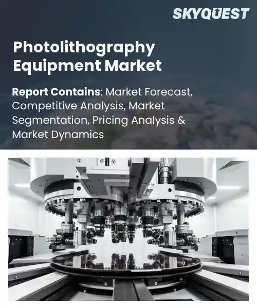
Photolithography Equipment Market
Report ID: SQMIG45N2208
Report ID: SQMIG45N2208
[email protected]
USA +1 351-333-4748
Report ID:
SQMIG45N2208 |
Region:
Global |
Published Date: May, 2026
Pages:
157
|Tables:
177
|Figures:
79


Global Photolithography Equipment Market size was valued at USD 15.3 Billion in 2024 and is poised to grow from USD 16.52 Billion in 2025 to USD 30.58 Billion by 2033, growing at a CAGR of 8.0% during the forecast period (2026-2033).
The photolithography equipment market centers on machines that transfer circuit patterns onto silicon wafers and is the technological linchpin of semiconductor manufacturing, enabling smaller, faster and more power-efficient chips. Its primary driver is the relentless demand for higher transistor density driven by Moore’s Law and surging compute needs for smartphones, cloud services and artificial intelligence, which forces fabs to adopt extreme ultraviolet (EUV) and advanced deep ultraviolet (DUV) systems.
Over decades the market evolved from contact and i-line steppers to sophisticated 193 nm immersion and EUV scanners, exemplified by ASML’s domination of EUV supply and investments by TSMC and Samsung.Building on node-driven equipment adoption, a critical factor shaping global market dynamics is capital intensity, because the high cost and long lead time of EUV scanners directly translate into concentrated supplier power, extended delivery backlogs and elevated wafer fabrication investment cycles.
As hyperscale and automotive customers require advanced nodes for AI inference, security and reliability, foundries increase tool orders which causes manufacturers to prioritize capacity expansion and aftermarket service offerings. Consequently suppliers gain recurring revenue from maintenance, upgrades and DUV refurbishment while governments’ incentive programs and demand for heterogeneous packaging create new markets for stepper-based lithography in advanced packaging production.
How is AI improving yield in the photolithography equipment market?
AI is improving yield in the photolithography equipment industry by bringing software driven intelligence to patterning and inspection. Key aspects are computational lithography for correction, machine learning for inline metrology and defect classification, and closed loop process control that tunes focus overlay and exposure in real time. Today leading tool makers and fabs are embedding AI models into scanner workflows and metrology chains to reduce rework and accelerate ramp of new nodes. This shift matters because growing demand for advanced chips is making smarter adaptive equipment a strategic advantage for vendors and manufacturers.
imec March 2026, received an ASML High NA EUV system that is being used to develop AI driven control and metrology flows. That capability supports yield improvement by enabling more accurate patterning, faster root cause analysis and richer training data for models so fabs can reduce defects and bring production online more quickly.
Market snapshot - 2026-2033
Global Market Size
USD 15.3 Billion
Largest Segment
Deep Ultraviolet (DUV) Lithography
Fastest Growth
Extreme Ultraviolet (EUV) Lithography
Growth Rate
8.0% CAGR
To get more insights on this market click here to Request a Free Sample Report
Global photolithography equipment market is segmented by technology, equipment type, light source, application, node size, end user and region. Based on technology, the market is segmented into Ultraviolet (UV) Lithography, Deep Ultraviolet (DUV) Lithography and Extreme Ultraviolet (EUV) Lithography. Based on equipment type, the market is segmented into ArF Immersion Lithography, ArF Dry Lithography, KrF Lithography, i-Line Lithography and Mask Aligners. Based on light source, the market is segmented into Mercury Lamps, Excimer Lasers and EUV Plasma Sources. Based on application, the market is segmented into Semiconductor Manufacturing, MEMS Manufacturing, Advanced Packaging, LED Manufacturing and Display Panel Manufacturing. Based on node size, the market is segmented into Below 7nm, 7nm–28nm and Above 28nm. Based on end user, the market is segmented into Integrated Device Manufacturers (IDMs), Foundries, Outsourced Semiconductor Assembly & Test (OSAT) Providers, Research Institutes and Others. Based on region, the market is segmented into North America, Europe, Asia Pacific, Latin America and Middle East & Africa.
EUV lithography segment leads with large photolithography equipment market because it enables the patterning fidelity and feature scaling that conventional optical systems cannot sustain, driving equipment manufacturers to prioritize EUV-capable steppers and factory investments. Superior resolution reduces complex multi-patterning requirements and simplifies integration, which channels vendor R&D and capital toward advanced optics, mask handling, and process control innovations that address escalating technical barriers and customer needs for next-generation nodes.
As per photolithography equipment market outlook, DUV lithography is emerging as the most rapidly expanding area because it underpins production for many mature node ranges and advanced packaging workflows. Improvements in immersion optics and laser sources, together with a substantial installed base and continuous vendor innovation, accelerate equipment upgrades and broader adoption, opening significant near-term opportunities across diverse manufacturing applications.
As per photolithography equipment market forecast, ArF immersion lithography segment is well-positioned in terms of developing high-volume manufacturing (HVM) capacity at advanced mainstream nodes, based on the combination of the overall resolution characteristics of the technology and its pragmatic focus of providing an efficient means for achieving cost-effective scaling from HVM facilities. The development of a mature process ecosystem and incremental improvements in equipment performance also enable equipment suppliers to further improve productivity while managing TCO which ultimately provides an ongoing justification for maintaining a stable demand for new equipment and services across logic and memory production and for continually refining existing tools and expanding service offerings.
As per photolithography equipment market analysis, mask aligners segment, on the other hand, is being driven by a significant increase in the volume of mask aligner systems being sold, as a result of the growing demand for R&D work, MEMS prototyping, LED fabrication, and low-cost packaged lines. In addition, enhanced automation and alignment accuracy, as well as hybrid exposure capabilities, have greatly increased the applicability of production masks across all production aspects of semiconductor-device manufacturing. As a result of these changes, many smaller HVM plants and laboratories are utilizing new mask aligners and will continue to drive new aftermarket services and specialized tool developments for mask aligners.
To get detailed segments analysis, Request a Free Sample Report
As per photolithography equipment industry analysis, Asia Pacific region has the largest market share due to its large concentration of semiconductor manufacturing facilities, complex integrated supply chains and longstanding commitment to invest in advanced fabrication technology. The high volume of business conducted by large foundries and memory manufacturers in the Asia Pacific region generates a near constant demand for state-of-the-art lithography equipment. Equipment vendors from Asia, Europe, and North America work closely with customers to accelerate the pace of technology adoption. There is an ample supply of specialized components manufacturers and metrology company's that support high yielding machine uptime. All of which create a very low level of production risk for end users of fab equipment.
In addition, because of the extremely close geographical proximity between the design and manufacture of wafer fabrication systems, it is possible to enhance the efficiency of both production processes and individual machines through iterative process improvements and custom tool designs. As such, the Asia Pacific region will continue to be the nexus of innovation and demand for services related to photolithography technology.
As per photolithography equipment market regional forecast, Japan leverages its already well-established precision machinery sector and extensive supply chain to gain an advantage in regards to the development of advanced photolithography equipment. Japanese equipment manufacturers partner with their domestic fabrication companies and nearby research institutions to prototype innovative optical systems and improve control of the lithography process. In addition, equipment service organizations provide fast and effective support of newly created photolithography equipment through their extensive service networks. The focus on innovative designs and high reliability continues to drive the demand for specialized photolithography systems needed for very sophisticated semiconductor fabrication applications and for high-value semiconductors sold domestically and internationally.
As per photolithography equipment market regional outlook, South Korea combines robust semiconductor manufacturing capabilities with proactive industry collaboration to drive equipment uptake. Large scale fabrication clusters maintain continuous engagement with equipment suppliers to co optimize processes and tailor tool specifications. A focus on high throughput production, close ties between design and manufacturing, and strong after sales support encourage rapid adoption of advanced lithography technologies tailored to memory and logic production pathways and export initiatives.
North America photolithography equipment industry is rapidly growing primarily fuelled by increasing domestic fabrication efforts as well as the presence of a large research community involved in this area, with many photolithography equipment manufacturer supplier partnerships to offer photolithograph equipment for domestic purposes. Partnerships between supply chain participants, such as universities and national laboratories, are having positive effects on reducing product development timelines for new photolithography technology and ultimately bringing it to market.
U.S. market has a diverse ecosystem comprised of semiconductor designers, advanced research institutions and well-established photolithography manufacturers that enable close collaboration between the photolithography equipment supplier and end users of photolithography equipment. Furthermore, there is a strong focus on research and development of innovations in process automation, metrology and process control through software solutions to improve upon the production of customized photolithography solutions.
Canada market is developing quickly and is making the correct investments in research driven innovations through strong partnerships between universities and industry to provide advanced manufacturing services to complement the fabrication of products by equipment distributors, system integrators and service suppliers. There is a strong emphasis on developing a qualified workforce and creating pathways to find technical support will lead to more equipment being used, while being close to the majority of the supply chain gives photolithography equipment suppliers and their customers quicker access to components, maintenance and consulting and export opportunities than other parts of the world.
European market is continuing to strengthen due to increased investment by researchers and manufacturers in their ability to provide cutting-edge solutions through both physical and intellectual partnerships, while at the same time providing strong partnerships between researchers, manufacturers and end-users of the equipment. Companies are putting great emphasis on precision engineering, metrology capabilities and the development of processes that use niche-level processing technologies to deliver new types of lithography systems specifically designed for automotive, industrial and power electronics markets. Cross-border technology collaborations and governmental support for the construction of a semiconductor supply chain are helping bridge the gaps in both components and skilled workers, thus providing a more complete manufacturing process. Manufacturers and system integrators across Europe are focused on providing modular, maintainable equipment and a strong after-market ecosystem as well as creating technology alliances with global companies to create an institutional environment for rapid technology transfer and modification to meet regional fabrication requirements; thus enhancing the European region's contribution to the market. Through targeted workforce development initiatives, standardizing of equipment-related metrics, and the establishment of pilot fabrication facilities, manufacturers in the region are accelerating the introduction of new products to market and providing the infrastructure required for the development of specialized domestic supply chains.
Photolithography equipment market in Germany benefits from a long standing tradition in precision engineering and strong ties between equipment manufacturers and industrial end users. Emphasis on robust, serviceable tool design, metrology integration and automation aligns with needs of automotive semiconductor producers. Close collaboration with technical universities facilitates process optimization and pilot production, while a dense network of suppliers and service providers ensures reliable maintenance, calibration and support for complex lithography systems.
United Kingdom research community is comprised of some of the best researchers in their field and has established a vibrant innovation ecosystem for developing new products and services. Strong working relationships between universities and the private sector promote the development of specialty technologies into products and measurement solutions. The concentration of suppliers and system integrators enables customized tooling and fast prototype production; furthermore, skills development and collaborative test facilities will help provide an avenue for products to reach market and to build supply chain connections.
France photolithography equipment market is another leading region in the world for research in optics, material science, and microfabrication with strong working relationships between research facilities and specialty equipment manufacturers. Specialty application areas such as power electronics and compound semiconductors are driving growth for customized lithographic equipment and measuring/characterizing technology. Supporting industrial policy, technical assistance networks and export-oriented producers will enhance the commercialization of innovative products created in Europe and increase collaboration within the continental European ecosystem.
To know more about the market opportunities by region and country, click here to
Buy The Complete Report
Advancements In EUV Technology
Rising Demand For Advanced Nodes
High Capital Expenditure Requirements
Complex Supply Chain Challenges
Request Free Customization of this report to help us to meet your business objectives.
Competitive dynamics in the global photolithography equipment market revolve around EUV scale up and DUV performance, prompting deals to secure optics and source technology, strategic co investments, and rapid module innovation. Vendors pursue acquisitions and partnerships to control bottlenecks; examples include ASML’s acquisition of Cymer, its long running collaboration with ZEISS, and customer co investment programs with Intel, Samsung and TSMC.
SkyQuest’s ABIRAW (Advanced Business Intelligence, Research & Analysis Wing) is our Business Information Services team that Collects, Collates, Correlates, and Analyses the Data collected by means of Primary Exploratory Research backed by robust Secondary Desk research.
As per SkyQuest analysis, the global photolithography equipment market growth is driven chiefly by relentless demand for higher transistor density and advanced nodes, which is one key driver pushing fabs toward EUV and advanced DUV systems. One restraint is the substantial capital expenditure tied to state of the art scanners, which concentrates purchases among well capitalized players and slows broader adoption. Asia Pacific remains the dominating region due to concentrated manufacturing capacity and integrated supply chains, while EUV lithography leads as the dominating segment because of superior resolution and node enabling capability. A second driver is AI enabled process control and computational lithography improving yield and ramp efficiency, further accelerating tool adoption.
| Report Metric | Details |
|---|---|
| Market size value in 2024 | USD 15.3 Billion |
| Market size value in 2033 | USD 30.58 Billion |
| Growth Rate | 8.0% |
| Base year | 2024 |
| Forecast period | 2026-2033 |
| Forecast Unit (Value) | USD Billion |
| Segments covered |
|
| Regions covered | North America (US, Canada), Europe (Germany, France, United Kingdom, Italy, Spain, Rest of Europe), Asia Pacific (China, India, Japan, Rest of Asia-Pacific), Latin America (Brazil, Rest of Latin America), Middle East & Africa (South Africa, GCC Countries, Rest of MEA) |
| Companies covered |
|
| Customization scope | Free report customization with purchase. Customization includes:-
|
To get a free trial access to our platform which is a one stop solution for all your data requirements for quicker decision making. This platform allows you to compare markets, competitors who are prominent in the market, and mega trends that are influencing the dynamics in the market. Also, get access to detailed SkyQuest exclusive matrix.
Table Of Content
Executive Summary
Market overview
Parent Market Analysis
Market overview
Market size
KEY MARKET INSIGHTS
COVID IMPACT
MARKET DYNAMICS & OUTLOOK
Market Size by Region
KEY COMPANY PROFILES
Methodology
For the Photolithography Equipment Market, our research methodology involved a mixture of primary and secondary data sources. Key steps involved in the research process are listed below:
1. Information Procurement: This stage involved the procurement of Market data or related information via primary and secondary sources. The various secondary sources used included various company websites, annual reports, trade databases, and paid databases such as Hoover's, Bloomberg Business, Factiva, and Avention. Our team did 45 primary interactions Globally which included several stakeholders such as manufacturers, customers, key opinion leaders, etc. Overall, information procurement was one of the most extensive stages in our research process.
2. Information Analysis: This step involved triangulation of data through bottom-up and top-down approaches to estimate and validate the total size and future estimate of the Photolithography Equipment Market.
3. Report Formulation: The final step entailed the placement of data points in appropriate Market spaces in an attempt to deduce viable conclusions.
4. Validation & Publishing: Validation is the most important step in the process. Validation & re-validation via an intricately designed process helped us finalize data points to be used for final calculations. The final Market estimates and forecasts were then aligned and sent to our panel of industry experts for validation of data. Once the validation was done the report was sent to our Quality Assurance team to ensure adherence to style guides, consistency & design.
Analyst Support
Customization Options
With the given market data, our dedicated team of analysts can offer you the following customization options are available for the Photolithography Equipment Market:
Product Analysis: Product matrix, which offers a detailed comparison of the product portfolio of companies.
Regional Analysis: Further analysis of the Photolithography Equipment Market for additional countries.
Competitive Analysis: Detailed analysis and profiling of additional Market players & comparative analysis of competitive products.
Go to Market Strategy: Find the high-growth channels to invest your marketing efforts and increase your customer base.
Innovation Mapping: Identify racial solutions and innovation, connected to deep ecosystems of innovators, start-ups, academics, and strategic partners.
Category Intelligence: Customized intelligence that is relevant to their supply Markets will enable them to make smarter sourcing decisions and improve their category management.
Public Company Transcript Analysis: To improve the investment performance by generating new alpha and making better-informed decisions.
Social Media Listening: To analyze the conversations and trends happening not just around your brand, but around your industry as a whole, and use those insights to make better Marketing decisions.
REQUEST FOR SAMPLE
 REQUEST FREE CUSTOMIZATION
Global Photolithography Equipment Market size was valued at USD 15.3 Billion in 2024 and is poised to grow from USD 16.52 Billion in 2025 to USD 30.58 Billion by 2033, growing at a CAGR of 8.0% during the forecast period (2026-2033).
Competitive dynamics in the global photolithography equipment market revolve around EUV scale up and DUV performance, prompting deals to secure optics and source technology, strategic co investments, and rapid module innovation. Vendors pursue acquisitions and partnerships to control bottlenecks; examples include ASML’s acquisition of Cymer, its long running collaboration with ZEISS, and customer co investment programs with Intel, Samsung and TSMC. 'ASML Holding N.V.', 'Canon Inc.', 'Nikon Corporation', 'Tokyo Electron Limited', 'Applied Materials, Inc.', 'Lam Research Corporation', 'KLA Corporation', 'SCREEN Holdings Co., Ltd.', 'Veeco Instruments Inc.', 'ULVAC, Inc.', 'SUSS MicroTec SE', 'EV Group', 'Hitachi High-Tech Corporation', 'SMEE', 'Onto Innovation Inc.', 'Rudolph Technologies', 'Zeiss Group', 'Intel Corporation', 'Taiwan Semiconductor Manufacturing Company', 'Samsung Electronics Co., Ltd.'
EUV lithography advancements enable finer feature patterning and improved yield, which encourages semiconductor manufacturers to invest in new equipment. As tool performance and process maturity improve, fabs can achieve higher integration densities and better performance in chips, prompting demand for equipment upgrades and capacity additions. The perception of reduced technical risk and clearer roadmap for next generation nodes makes procurement decisions more confident, driving vendors to scale production and innovate complementary modules, thereby reinforcing market adoption and stimulating further development of photolithography systems.
Euv And High Na Advancement: Industry momentum toward extreme ultraviolet and high numerical aperture platforms is redefining resolution limits and enabling next generation logic and memory nodes. Equipment suppliers are focusing on optical innovation, source power, and mask technologies while foundries and design houses align process flows. This trend stimulates ecosystem partnerships, specialized service offerings, and novel process integration strategies that prioritize yield management and pattern fidelity, driving demand for precision metrology and iterative collaborative development across the value chain at scale globally and rapidly.
Why does Asia Pacific Dominate the Global Photolithography Equipment Market? |@12


Want to customize this report? This report can be personalized according to your needs. Our analysts and industry experts will work directly with you to understand your requirements and provide you with customized data in a short amount of time. We offer $1000 worth of FREE customization at the time of purchase.
Feedback From Our Clients


 USA (+1) 351-333-4748

