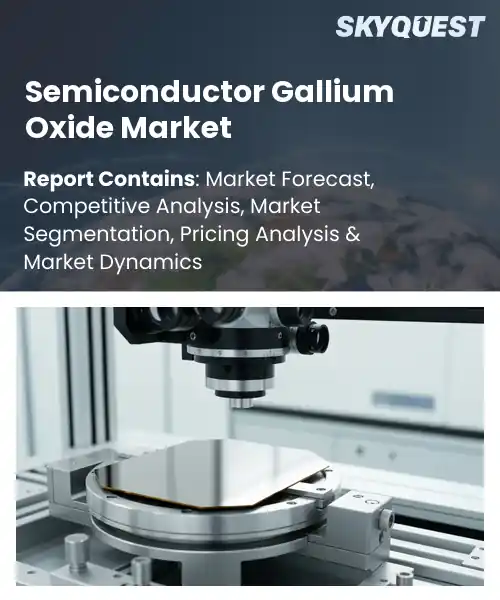
Semiconductor Gallium Oxide Market
Report ID: SQMIG45O2096
Report ID: SQMIG45O2096
sales@skyquestt.com
USA +1 351-333-4748
Report ID:
SQMIG45O2096 |
Region:
Global |
Published Date: February, 2026
Pages:
157
|Tables:
142
|Figures:
78


Global Semiconductor Gallium Oxide Market size was valued at USD 14.3 Billion in 2024 and is poised to grow from USD 18.76 Billion in 2025 to USD 164.72 Billion by 2033, growing at a CAGR of 31.2% during the forecast period (2026-2033).
The semiconductor gallium oxide market is driven by the need for higher-voltage, higher-efficiency power devices that silicon and wide-bandgap materials struggle to achieve. As an ultra-wide-bandgap material, gallium oxide enables devices with much higher breakdown fields and potentially lower on-resistance, which matters for power conversion in electric vehicles, renewable energy inverters, data center power supplies and high-voltage transmission. The market has evolved from academic demonstrations to commercialization, with research groups and device makers scaling wafer production and demonstrating prototype MOSFETs and Schottky diodes. This developmental trajectory reflects a transition from laboratory feasibility to targeted industrial adoption across demanding power applications.Building on its material advantages, a key growth factor for the global gallium oxide market is the commercialization of native substrates and epitaxial processes, because lower-cost, larger-area wafers directly reduce device cost and enable manufacturing. As substrate suppliers scale and yield improves, device makers can produce MOSFETs and diodes suited for ultra-high-voltage applications, which creates demand from electric vehicle fast chargers, HVDC links and industrial motor drives. Concurrent regulatory pressure to improve energy efficiency accelerates adoption since Ga2O3 devices can cut conduction and switching losses, thereby lowering system operating costs and opening opportunities for integrated power modules and high-reliability aerospace electronics.
Recent market developments underscore significant shifts in semiconductor gallium oxide market sector dynamics. PowerCubeSemi announced a successful pre IPO funding round in December 2025, accelerating its KOSDAQ listing plans and highlighting progress toward commercial gallium oxide products such as deep ultraviolet sensors and multi kilovolt power devices, reinforcing the companys position as a developer of production scale Ga2O3 wafers and devices for automotive
How is AI accelerating gallium oxide semiconductor device development?
AI is speeding gallium oxide semiconductor development by improving materials discovery, process control, device modeling, and yield management. Machine learning models help predict defect formation and guide substrate and epitaxy recipe choices. Data driven process optimization shortens experimental cycles and reduces costly trial and error. In fabrication, AI driven inspection and predictive maintenance increase throughput and reliability. Market context shows growing demand for higher voltage and energy efficient power devices and strong competition from other wide bandgap materials, so faster, lower risk scale up makes gallium oxide more commercially attractive. Examples include AI aided simulation for interatomic potentials and automated fab analytics.Mingjia Semiconductor, February 2026, reported expanded mass production and wafer shipments, demonstrating how AI driven simulation and closed loop process control shorten development cycles and raise effective yield, which supports faster commercialization and broader market adoption for gallium oxide devices.
Market snapshot - (2026-2033)
Global Market Size
USD 14.3 Billion
Largest Segment
Thin Film Ga2O3
Fastest Growth
Nanowire Ga2O3
Growth Rate
31.2% CAGR
To get more insights on this market click here to Request a Free Sample Report
Global semiconductor gallium oxide market is segmented by material type, form factor, production method, application, end-user industry and region. Based on material type, the market is segmented into Thin Film Ga2O3 and Nanowire Ga2O3. Based on form factor, the market is segmented into Discreet Devices and Integrated Circuits. Based on production method, the market is segmented into MOCVD, HVPE and Sputtering. Based on application, the market is segmented into Power Electronics, Photonics and Electronic Devices. Based on end-user industry, the market is segmented into Automotive, Telecommunications and Consumer Electronics. Based on region, the market is segmented into North America, Europe, Asia Pacific, Latin America and Middle East & Africa.
Thin Film Ga2O3 segment dominates because its wafer-scale epitaxial films provide the uniformity and crystalline quality needed for reliable high-voltage devices. Lower defect densities and stable electrical behavior reduce design risk for manufacturers, speeding integration into power architectures. Compatibility with established deposition and lithography workflows enables predictable process transfer, creating a practical pathway from laboratory prototypes to commercially manufacturable products. That manufacturability advantage attracts supply chain and equipment investment.
Thin Film Ga2O3 adoption expands the market by enabling scalable wafer-level manufacturing that lowers unit costs and strengthens supply confidence. Broad industry uptake attracts tooling and material suppliers, which accelerates commercialization cycles and unlocks new device opportunities, thereby creating business growth across the semiconductor value chain.
MOCVD segment leads because its vapor phase epitaxy approach enables controlled layer-by-layer growth with fine control over stoichiometry and thickness, which directly improves film uniformity across larger wafers. Process automation and mature reactor designs support repeatable throughput, reducing variability that otherwise hampers scale-up. As a result, manufacturers can translate material improvements into consistent device yields, making MOCVD the preferred path for scaling gallium oxide from research to production.
MOCVD-driven scalability accelerates market growth by enabling consistent throughput and yields, which lower manufacturing risk and attract capital investment. Mature processes support supply chain commitment and allow device makers to plan product roadmaps with confidence, creating commercial opportunities and expanding application adoption that drives demand for gallium oxide components.
To get detailed segments analysis, Request a Free Sample Report
Asia Pacific dominance is rooted in a concentrated ecosystem that integrates advanced materials research, device manufacturing and comprehensive supply chains. The region hosts a critical mass of electronics manufacturers, specialized component suppliers and academic institutions collaborating on gallium oxide epitaxy, device design and reliability testing. Strong industrial focus on high power and high frequency applications, coupled with proactive industrial strategies and localized pilot production capabilities, shortens development cycles and supports rapid commercialization. Proximity to fabrication, packaging and system integrators enables efficient scale up from prototypes to production. This convergence of technical expertise, manufacturing depth and collaborative networks reinforces Asia Pacific leadership in advancing gallium oxide technologies and translating innovations into commercially viable devices for diverse end use sectors.
Semiconductor Gallium Oxide Market in Japan is characterized by close collaboration between precision electronics manufacturers and leading research centers, emphasizing material quality, process integration and device reliability. Domestic firms focus on high precision production and advanced testing protocols, while academic institutions drive foundational research in epitaxial growth and defect control. Policy frameworks and industry coordinated initiatives encourage pilot production and technology transfer, enabling Japanese contributors to shape standards and deliver high value components for specialized applications within regional supply chains.
Semiconductor Gallium Oxide Market in South Korea benefits from a dynamic electronics supply chain, strong private sector investment and emphasis on scaling manufacturing for advanced power devices. Large conglomerates and specialized suppliers partner with research institutes to refine growth techniques and fabrication processes, while advanced packaging and system integration capabilities support deployment in telecom and automotive applications. This industrial alignment accelerates commercialization pathways and positions South Korea as a key adopter and industrial collaborator within the Asia Pacific gallium oxide landscape.
The rapid expansion in North America is driven by a robust innovation ecosystem that blends cutting edge research, specialized foundries and application driven industry demand. Cross sector collaboration targets defense, telecommunications and clean energy systems that require high performance power and RF components, creating demand for alternative wide bandgap materials like gallium oxide. Strategic initiatives to diversify supply chains and strengthen domestic development capabilities have stimulated partnerships between industry, national laboratories and universities. Emphasis on commercialization pathways, pilot production infrastructure and reliability validation supports transition from laboratory innovations to marketable devices. This combination of application demand, research depth and industry driven development positions North America as an important growth region for gallium oxide technologies and related manufacturing capabilities.
Semiconductor Gallium Oxide Market in United States is shaped by a vibrant innovation landscape combining leading research institutions, specialized fabrication facilities and application focused end users. Collaborative programs between industry and national laboratories advance materials development and device testing, while private investment supports prototype scaling and pilot production efforts. Strong demand from defense, telecom and industrial sectors drives application oriented development and reliability validation, positioning United States as a primary node for commercialization, standards development and technology integration in the broader North American market.
Semiconductor Gallium Oxide Market in Canada leverages concentrated research strengths and innovation programs that support advanced materials and device prototyping. University laboratories and research centers collaborate with industry partners to refine epitaxy techniques and testing frameworks, focusing on niche high performance applications and sensor integration. Cross border partnerships and regional collaboration enable complementary pilot production and validation capabilities, establishing Canada as an important contributor to research driven development and early commercialization activities within the North American gallium oxide ecosystem.
Europe is strengthening its position through coordinated initiatives that emphasize research collaboration, industrial modernization and strategic supply chain development. Regional clusters bring together research institutions, specialized manufacturers and end users to advance material science, epitaxial processes and device integration for power electronics and telecom applications. Emphasis on sustainable manufacturing practices, standards development and pilot production facilities supports transition from research to demonstrated products. Public private partnerships and cross border consortia foster technology transfer and shared infrastructure, enabling European stakeholders to develop competitive capabilities, reduce dependency on external sources and support continental needs for high performance semiconductor components.
Semiconductor Gallium Oxide Market in Germany combines strong industrial engineering expertise with close ties to automotive and industrial electronics sectors. Research institutes collaborate with manufacturers to improve material processing, device reliability and system integration for high voltage and powertrain applications. A focus on manufacturing precision, quality assurance and supply chain resilience underpins efforts to develop industrial grade gallium oxide components, while collaborative projects facilitate technology transfer from laboratories to pilot production within the German industrial ecosystem.
Semiconductor Gallium Oxide Market in United Kingdom benefits from academic excellence and a growing cluster of specialized startups focused on materials science and device prototyping. University led research, supported test facilities and investment networks promote early stage commercialization and validation of gallium oxide technologies for telecom and defense applications. Policy emphasis on innovation and international collaboration helps translate research outcomes into marketable products, positioning United Kingdom as a hub for early commercialization and cross border partnership within European supply chains.
Semiconductor Gallium Oxide Market in France is shaped by strong public research institutions and industrial players focusing on power electronics and system level integration. Concentration on advanced epitaxial techniques, device packaging and reliability testing supports integration of gallium oxide into high performance applications. National initiatives encourage partnerships between research centers and manufacturers to accelerate prototype development and demonstration projects, reinforcing France role in the broader European effort to build strategic semiconductor capabilities.
To know more about the market opportunities by region and country, click here to
Buy The Complete Report
Technological Advancements In Materials
Growing Demand For Power Electronics
High Manufacturing Complexity and Costs
Limited Substrate Availability was Constraining
Request Free Customization of this report to help us to meet your business objectives.
Competitive landscape centers on rapid vertical integration, substrate-to-device partnerships, and government-backed pilot consortia that accelerate commercialization. Material suppliers and device startups pursue partnerships and licensing to lock technical roadmaps; for example Kyma Technologies and Novel Crystal Technology linked epi growth and substrate supply to scale Ga2O3 wafers, while university spinouts leverage DoD and NSF programs to finance device prototyping.
Top Player’s Company Profile
Recent Developments
Energy Efficiency In Power Systems: Adoption of gallium oxide materials is driven by demand for efficient power conversion across industrial applications. Designers prioritize lower switching losses, improved thermal resilience, and compact form factors to meet tightening energy targets and system miniaturization. This trend encourages collaboration among material scientists, device manufacturers, and systems integrators to optimize gallium oxide components for broader real-world deployments. As stakeholders seek longer lifecycle performance and reduced energy consumption, gallium oxide positions itself as a compelling alternative to traditional wide bandgap technologies.
High-Frequency Communications Expansion: Growing demand for advanced wireless infrastructure and connectivity is creating opportunities for gallium oxide in radio frequency applications. Its material properties enable devices that support higher power density and thermal stability, attractive for base stations, satellite payloads, and radar systems. Industry participants are exploring device design adaptations and packaging improvements to integrate gallium oxide into RF ecosystems. Partnerships between telecom operators, equipment vendors, and semiconductor firms are accelerating application specific development and piloting of gallium oxide solutions across commercial segments.
SkyQuest’s ABIRAW (Advanced Business Intelligence, Research & Analysis Wing) is our Business Information Services team that Collects, Collates, Correlates, and Analyses the Data collected by means of Primary Exploratory Research backed by robust Secondary Desk research. As per SkyQuest analysis, the global semiconductor gallium oxide market is propelled primarily by growing demand for energy-efficient, high-voltage power electronics, while a second important driver is rapid advances in crystal growth and epitaxial techniques that improve material quality and manufacturability. However, high manufacturing complexity and costs remain a key restraint, slowing investment and scale-up despite clear system benefits. Asia Pacific leads the market due to its integrated research, manufacturing and supply chain ecosystem, and Thin Film Ga2O3 is the dominating segment because wafer-scale epitaxy delivers the uniformity and process compatibility needed for commercial high-voltage devices. This convergence positions gallium oxide as a strategic option for EV charging, renewable inverters and industrial power systems.
| Report Metric | Details |
|---|---|
| Market size value in 2024 | USD 14.3 Billion |
| Market size value in 2033 | USD 164.72 Billion |
| Growth Rate | 31.2% |
| Base year | 2024 |
| Forecast period | (2026-2033) |
| Forecast Unit (Value) | USD Billion |
| Segments covered |
|
| Regions covered | North America (US, Canada), Europe (Germany, France, United Kingdom, Italy, Spain, Rest of Europe), Asia Pacific (China, India, Japan, Rest of Asia-Pacific), Latin America (Brazil, Rest of Latin America), Middle East & Africa (South Africa, GCC Countries, Rest of MEA) |
| Companies covered |
|
| Customization scope | Free report customization with purchase. Customization includes:-
|
To get a free trial access to our platform which is a one stop solution for all your data requirements for quicker decision making. This platform allows you to compare markets, competitors who are prominent in the market, and mega trends that are influencing the dynamics in the market. Also, get access to detailed SkyQuest exclusive matrix.
Table Of Content
Executive Summary
Market overview
Parent Market Analysis
Market overview
Market size
KEY MARKET INSIGHTS
COVID IMPACT
MARKET DYNAMICS & OUTLOOK
Market Size by Region
KEY COMPANY PROFILES
Methodology
For the Semiconductor Gallium Oxide Market, our research methodology involved a mixture of primary and secondary data sources. Key steps involved in the research process are listed below:
1. Information Procurement: This stage involved the procurement of Market data or related information via primary and secondary sources. The various secondary sources used included various company websites, annual reports, trade databases, and paid databases such as Hoover's, Bloomberg Business, Factiva, and Avention. Our team did 45 primary interactions Globally which included several stakeholders such as manufacturers, customers, key opinion leaders, etc. Overall, information procurement was one of the most extensive stages in our research process.
2. Information Analysis: This step involved triangulation of data through bottom-up and top-down approaches to estimate and validate the total size and future estimate of the Semiconductor Gallium Oxide Market.
3. Report Formulation: The final step entailed the placement of data points in appropriate Market spaces in an attempt to deduce viable conclusions.
4. Validation & Publishing: Validation is the most important step in the process. Validation & re-validation via an intricately designed process helped us finalize data points to be used for final calculations. The final Market estimates and forecasts were then aligned and sent to our panel of industry experts for validation of data. Once the validation was done the report was sent to our Quality Assurance team to ensure adherence to style guides, consistency & design.
Analyst Support
Customization Options
With the given market data, our dedicated team of analysts can offer you the following customization options are available for the Semiconductor Gallium Oxide Market:
Product Analysis: Product matrix, which offers a detailed comparison of the product portfolio of companies.
Regional Analysis: Further analysis of the Semiconductor Gallium Oxide Market for additional countries.
Competitive Analysis: Detailed analysis and profiling of additional Market players & comparative analysis of competitive products.
Go to Market Strategy: Find the high-growth channels to invest your marketing efforts and increase your customer base.
Innovation Mapping: Identify racial solutions and innovation, connected to deep ecosystems of innovators, start-ups, academics, and strategic partners.
Category Intelligence: Customized intelligence that is relevant to their supply Markets will enable them to make smarter sourcing decisions and improve their category management.
Public Company Transcript Analysis: To improve the investment performance by generating new alpha and making better-informed decisions.
Social Media Listening: To analyze the conversations and trends happening not just around your brand, but around your industry as a whole, and use those insights to make better Marketing decisions.
REQUEST FOR SAMPLE
 REQUEST FREE CUSTOMIZATION


Want to customize this report? This report can be personalized according to your needs. Our analysts and industry experts will work directly with you to understand your requirements and provide you with customized data in a short amount of time. We offer $1000 worth of FREE customization at the time of purchase.
Feedback From Our Clients

 USA (+1) 351-333-4748
