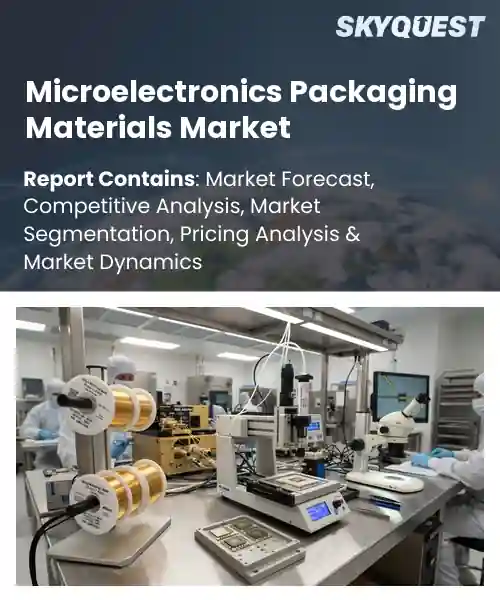
Microelectronics Packaging Materials Market
Report ID: SQMIG45K2468
Report ID: SQMIG45K2468
[email protected]
USA +1 351-333-4748
Report ID:
SQMIG45K2468 |
Region:
Global |
Published Date: September, 2026
Pages:
157
|Tables:
126
|Figures:
77


Global Microelectronics Packaging Materials Market size was valued at USD 6.94 Billion in 2024 and is poised to grow from USD 7.47 Billion in 2025 to USD 13.42 Billion by 2033, growing at a CAGR of 7.6% during the forecast period (2026-2033).
The global microelectronics packaging materials market supplies the substrates, die‑attach adhesives, encapsulants and underfills that protect and interconnect semiconductor chips. Its importance stems from the relentless demand for smaller, faster and more reliable electronic devices, a trend that fuels constant innovation in packaging. Historically the market evolved from simple epoxy molds in the 1970s to advanced organic substrates and copper‑core laminates that support high‑frequency communication and automotive power modules. For instance, the shift to 5G smartphones drove the adoption of low‑loss dielectric materials, while electric‑vehicle power converters required thermally conductive adhesives. This evolution illustrates how performance pressures reshape material selection. The dominant growth factor is the convergence of packaging architectures such as system‑in‑package (SiP) and fan‑out wafer‑level packaging (FOWLP) with material science, because these designs demand thinner, more stable and insulating substrates. As manufacturers adopt SiP for wearables, need for interposers made from organic‑core laminates rises, prompting suppliers to invest in low‑CTE (coefficient of thermal expansion) polymers that mitigate warpage. This investment creates opportunities for players specializing in epoxy‑based underfills that can endure the thermal cycling of vehicle processors. Consequently, the market expands not only through volume growth but also via pricing for materials that unlock integration levels and reliability.
How is AI-driven automation shaping the microelectronics packaging materials market?
AI-driven automation is redefining how microelectronics packaging materials are produced and applied. By integrating machine‑learning models with robotic handling, manufacturers can predict material behavior, optimize curing cycles, and adjust process parameters in real time. This reduces defects, shortens time‑to‑market, and enables the use of advanced substrates that support higher device density. The market is shifting toward smart factories where data from sensors guides the selection of underfills, encapsulants, and interposers, ensuring consistent performance across increasingly complex packages. Early adopters report smoother workflow, lower waste, and the ability to scale production without sacrificing quality, making automation a core growth catalyst.Recent industry activity highlights the impact of AI‑enabled lines, with a leading packaging supplier launching an automated material‑handling system in June 2024, accelerating throughput and improving yield while cutting manual intervention. This innovation showcases how intelligent automation fuels efficiency and supports the market’s expansion.
Market snapshot - (2026-2033)
Global Market Size
USD 6.94 Billion
Largest Segment
Substrate Materials
Fastest Growth
Underfill Materials
Growth Rate
7.6% CAGR
To get more insights on this market click here to Request a Free Sample Report
Global microelectronics packaging materials market is segmented by material type, packaging type, application, end user and region. Based on material type, the market is segmented into Encapsulants, Die Attach Materials, Underfill Materials, Leadframe Materials, Substrate Materials, Bonding Materials and Others. Based on packaging type, the market is segmented into Wire Bonding, Flip Chip, Wafer-Level Packaging, Chip-Scale Packaging and Others. Based on application, the market is segmented into Consumer Electronics, Automotive Electronics, Telecommunications, Industrial Electronics and Others. Based on end user, the market is segmented into Semiconductor Manufacturers, Electronics Manufacturers, Foundries and Others. Based on region, the market is segmented into North America, Europe, Asia Pacific, Latin America and Middle East & Africa.
Encapsulants segment dominates because it provides essential protection against moisture, mechanical stress, and thermal cycling, ensuring reliability of advanced semiconductor devices. The material’s ability to conform to increasingly fine pitch architectures and to integrate seamlessly with various interconnect technologies makes it indispensable. Growing demand for high performance consumer electronics and stringent reliability standards drive manufacturers to prioritize premium encapsulant solutions, reinforcing its central position in the market throughout the supply chain.
Meanwhile, Die Attach Materials segment emerges as the fastest growing area because high power and high frequency chips require adhesives that dissipate heat while maintaining electrical performance. Innovations in low k and lead free formulations open opportunities in automotive and telecom devices, accelerating market expansion and creating revenue streams.
Flip Chip segment leads because it enables direct electrical connections with minimal inductance, supporting higher data rates and power densities demanded by modern devices. Its ability to reduce package count and footprint aligns with trends toward miniaturization, while facilitating superior thermal paths that improve reliability. The convergence of consumer, automotive, and communication sectors on these performance attributes fuels sustained investment in flip chip compatible materials, cementing its leadership.
Conversely, Wafer Level Packaging segment is witnessing the strongest growth because it integrates multiple functions at the wafer stage, dramatically cutting assembly steps and cost. Advances in fan out technologies and material innovations enable thinner, lighter packages for IoT and high frequency applications, driving rapid adoption and expanding market horizons.
To get detailed segments analysis, Request a Free Sample Report
Asia Pacific leverages a confluence of deep semiconductor design expertise, high‑volume manufacturing capacity, and tightly integrated supply chains that accelerate innovation in packaging technologies. Major foundries and assembly houses cluster in this region, fostering collaboration and rapid iteration. Governments provide robust policy support and incentives that nurture research and development, while a skilled engineering workforce sustains continuous improvement. The proximity of component suppliers to end‑product manufacturers reduces lead times and enhances responsiveness to emerging device architectures. Consequently, the region consistently introduces advanced material solutions that align with evolving performance demands, reinforcing its leadership position in the global market.
Microelectronics Packaging Materials Market in Japan benefits from a legacy of precision engineering and strong ties between electronics manufacturers and material suppliers. Collaborative research initiatives between universities and industry drive the development of high‑performance substrates and interconnects. Emphasis on reliability and miniaturization aligns with domestic demand for automotive electronics and high‑end consumer devices, encouraging continual refinement of packaging material capabilities.
Microelectronics Packaging Materials Market in South Korea is propelled by a dynamic semiconductor ecosystem that prioritizes cutting‑edge packaging solutions. Close coordination between memory manufacturers and material innovators accelerates the adoption of advanced packaging formats. Government‑backed programs focus on material science breakthroughs, supporting the transition toward heterogeneous integration and high‑density interconnects, thereby strengthening the market’s competitive edge.
North America experiences robust expansion driven by strong demand for high‑performance computing, data center infrastructure, and emerging technologies such as artificial intelligence and autonomous systems. The region houses leading semiconductor design firms that require sophisticated packaging materials to meet stringent performance and reliability criteria. Significant investment in research collaborations between academia, industry, and government agencies fuels continuous material innovation. A focus on sustainable manufacturing practices and advanced recycling also shapes market dynamics, while a mature supply chain infrastructure ensures rapid adoption of next‑generation packaging solutions across diverse application sectors.
Microelectronics Packaging Materials Market in the United States is energized by a vibrant ecosystem of semiconductor designers and device manufacturers seeking ever‑greater integration density. Strategic partnerships between material suppliers and leading chip makers accelerate the rollout of advanced die‑to‑die and fan‑out technologies. Federal research initiatives and venture capital support prioritize material breakthroughs that enable higher bandwidth and lower power consumption, reinforcing the market’s growth trajectory.
Microelectronics Packaging Materials Market in Canada benefits from a strong focus on research excellence and collaborative innovation clusters. Universities and research institutes partner with material producers to explore novel dielectric and substrate solutions for emerging quantum and photonic devices. Government incentives encourage the commercialization of sustainable packaging materials, positioning Canada as a niche contributor to the broader North American market.
Europe strengthens its market position through coordinated industrial strategies that emphasize advanced material development, sustainability, and standards harmonization. Deep expertise in precision manufacturing and a rich network of research institutions drive the creation of high‑reliability packaging materials for automotive, aerospace, and industrial applications. Policy frameworks promote eco‑friendly material cycles and incentivize cross‑border collaboration, fostering a resilient ecosystem. Furthermore, Europe’s commitment to open standards facilitates interoperability and accelerates adoption of innovative packaging architectures across the continent, enhancing competitiveness on the global stage.
Microelectronics Packaging Materials Market in Germany capitalizes on its renowned engineering precision and strong automotive electronics sector. Close collaboration between material manufacturers and vehicle system suppliers drives the development of robust, thermally efficient packaging solutions. Emphasis on circular economy principles encourages the reuse and recycling of advanced substrates, aligning with broader sustainability goals.
Microelectronics Packaging Materials Market in the United Kingdom is shaped by vibrant research hubs that focus on next‑generation interconnects and high‑frequency materials. Partnerships between academic institutions and industry accelerate prototyping of innovative packaging formats for telecommunications and defense applications. Policy support for high‑tech manufacturing bolsters the market’s evolution.
Microelectronics Packaging Materials Market in France benefits from a strong focus on aerospace and defense electronics, where reliability and performance are paramount. Collaborative projects between material firms and aircraft system developers foster the creation of lightweight, high‑conductivity packaging solutions. National initiatives encourage the integration of sustainable material practices, reinforcing France’s role in the European landscape.
To know more about the market opportunities by region and country, click here to
Buy The Complete Report
Increasing Chip Complexity
Adoption Of Advanced Substrates
Rising Material Cost Pressures
Stringent Environmental Regulations
Request Free Customization of this report to help us to meet your business objectives.
The global microelectronics packaging materials market is intensely competitive, with major players leveraging strategic M&A, joint ventures, and rapid technology innovation to secure supply chain resilience and meet demand for higher performance interconnects; recent examples include ASE Group’s acquisition of a Dow advanced epoxy portfolio and Amkor Technology’s partnership with Intel to co‑develop fan‑out wafer‑level packaging, both aimed at expanding material capabilities and accelerating time‑to‑market.
Top Player’s Company Profile
Recent Developments
SkyQuest’s ABIRAW (Advanced Business Intelligence, Research & Analysis Wing) is our Business Information Services team that Collects, Collates, Correlates, and Analyses the Data collected by means of Primary Exploratory Research backed by robust Secondary Desk research. As per SkyQuest analysis the global microelectronics packaging materials market is projected to reach $13.42 billion by 2033, driven first by rising chip complexity that pushes designers to seek higher‑performance die‑attach, underfill and especially encapsulant solutions, while the adoption of advanced substrates such as organic and glass interposers adds a second growth engine by enabling finer line widths and better thermal paths. The encapsulants segment currently leads the market because it safeguards devices against moisture and thermal cycling. Asia Pacific dominates the landscape thanks to its dense semiconductor ecosystem and integrated supply chains. However, escalating material cost pressures act as a restraint, forcing manufacturers to balance performance with price.
| Report Metric | Details |
|---|---|
| Market size value in 2024 | USD 6.94 Billion |
| Market size value in 2033 | USD 13.42 Billion |
| Growth Rate | 7.6% |
| Base year | 2024 |
| Forecast period | (2026-2033) |
| Forecast Unit (Value) | USD Billion |
| Segments covered |
|
| Regions covered | North America (US, Canada), Europe (Germany, France, United Kingdom, Italy, Spain, Rest of Europe), Asia Pacific (China, India, Japan, Rest of Asia-Pacific), Latin America (Brazil, Rest of Latin America), Middle East & Africa (South Africa, GCC Countries, Rest of MEA) |
| Companies covered |
|
| Customization scope | Free report customization with purchase. Customization includes:-
|
To get a free trial access to our platform which is a one stop solution for all your data requirements for quicker decision making. This platform allows you to compare markets, competitors who are prominent in the market, and mega trends that are influencing the dynamics in the market. Also, get access to detailed SkyQuest exclusive matrix.
Table Of Content
Executive Summary
Market overview
Parent Market Analysis
Market overview
Market size
KEY MARKET INSIGHTS
COVID IMPACT
MARKET DYNAMICS & OUTLOOK
Market Size by Region
KEY COMPANY PROFILES
Methodology
For the Microelectronics Packaging Materials Market, our research methodology involved a mixture of primary and secondary data sources. Key steps involved in the research process are listed below:
1. Information Procurement: This stage involved the procurement of Market data or related information via primary and secondary sources. The various secondary sources used included various company websites, annual reports, trade databases, and paid databases such as Hoover's, Bloomberg Business, Factiva, and Avention. Our team did 45 primary interactions Globally which included several stakeholders such as manufacturers, customers, key opinion leaders, etc. Overall, information procurement was one of the most extensive stages in our research process.
2. Information Analysis: This step involved triangulation of data through bottom-up and top-down approaches to estimate and validate the total size and future estimate of the Microelectronics Packaging Materials Market.
3. Report Formulation: The final step entailed the placement of data points in appropriate Market spaces in an attempt to deduce viable conclusions.
4. Validation & Publishing: Validation is the most important step in the process. Validation & re-validation via an intricately designed process helped us finalize data points to be used for final calculations. The final Market estimates and forecasts were then aligned and sent to our panel of industry experts for validation of data. Once the validation was done the report was sent to our Quality Assurance team to ensure adherence to style guides, consistency & design.
Analyst Support
Customization Options
With the given market data, our dedicated team of analysts can offer you the following customization options are available for the Microelectronics Packaging Materials Market:
Product Analysis: Product matrix, which offers a detailed comparison of the product portfolio of companies.
Regional Analysis: Further analysis of the Microelectronics Packaging Materials Market for additional countries.
Competitive Analysis: Detailed analysis and profiling of additional Market players & comparative analysis of competitive products.
Go to Market Strategy: Find the high-growth channels to invest your marketing efforts and increase your customer base.
Innovation Mapping: Identify racial solutions and innovation, connected to deep ecosystems of innovators, start-ups, academics, and strategic partners.
Category Intelligence: Customized intelligence that is relevant to their supply Markets will enable them to make smarter sourcing decisions and improve their category management.
Public Company Transcript Analysis: To improve the investment performance by generating new alpha and making better-informed decisions.
Social Media Listening: To analyze the conversations and trends happening not just around your brand, but around your industry as a whole, and use those insights to make better Marketing decisions.
REQUEST FOR SAMPLE
 REQUEST FREE CUSTOMIZATION


Want to customize this report? This report can be personalized according to your needs. Our analysts and industry experts will work directly with you to understand your requirements and provide you with customized data in a short amount of time. We offer $1000 worth of FREE customization at the time of purchase.
Feedback From Our Clients


 USA (+1) 351-333-4748

