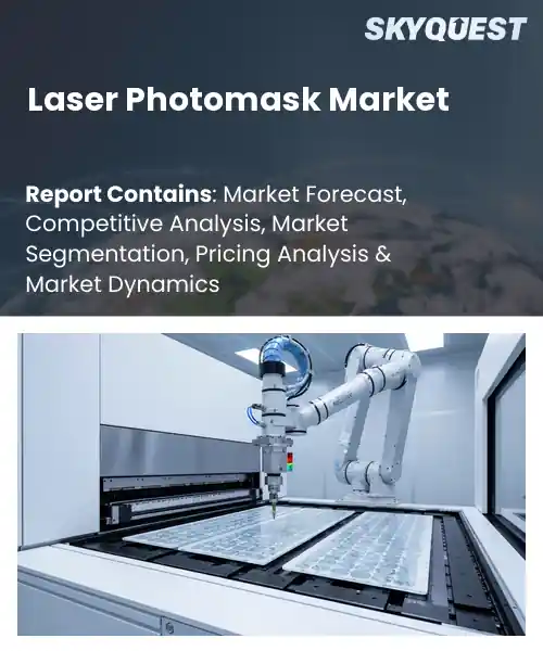
Laser Photomask Market
Report ID: SQMIG45N2252
Report ID: SQMIG45N2252
[email protected]
USA +1 351-333-4748
Report ID:
SQMIG45N2252 |
Region:
Global |
Published Date: July, 2026
Pages:
157
|Tables:
115
|Figures:
77


Global Laser Photomask Market size was valued at USD 3.66 Billion in 2024 and is poised to grow from USD 3.82 Billion in 2025 to USD 5.39 Billion by 2033, growing at a CAGR of 4.4% during the forecast period (2026-2033).
The laser photomask market has emerged as a critical enabler for advanced semiconductor fabrication, driven primarily by the relentless demand for smaller, faster chips. With the feature sizes falling under 10 nm, the traditional quartz masks are failing to provide the required overlay accuracy in extreme ultraviolet (EUV) lithography which has led manufacturers to switch to laser-written masks that can achieve a precision of less than one nanometer. Beginning in the early parts of 2010, companies like ASML and Toppan spent heavily on the manufacturing technology based on the concept of laser-direct-write and expanded the capabilities of this technology to be able to meet the requirements of high-volume production lines.
Another pivotal factor shaping the global laser photomask market is the rapid uptake of EUV lithography in high‑performance computing and mobile chips, which drives demand for masks that can survive higher photon flux while maintaining pattern fidelity. This necessity motivates investments in glass substrates with low thermal expansion and laser defect repair, which reduces the amount of defective yield. For example, Taiwan Semiconductor Manufacturing Company reported a 12% increase in wafer throughput after implementing lasers to write photomasks for its 5 nm technology node, showing cost efficiency. As a result, companies that apply a combination of lasers and AI inspections have a good opportunity to acquire substantial market shares as manufacturers want to shorten cycle times and reduce costs.
How is AI-Driven Automation Influencing Yield and Cost Efficiency in the Laser Photomask Market?
AI‑driven automation is reshaping laser photomask production by integrating real‑time defect detection, pattern optimization and process control into the lithography workflow. Machine‑learning models analyze inspection data instantly, allowing operators to correct mask defects before they propagate, which lifts overall yield. The same algorithms predict optimal laser exposure parameters, reducing material waste and shortening cycle time. Together these capabilities tighten tolerances, lower per‑mask cost and make high‑volume manufacturing more sustainable, positioning the market for steady expansion as chip designers demand finer patterns.
In June 2026, Lasertec Corporation highlighted its AI‑enhanced mask‑blank inspection platform, noting faster defect identification and reduced rework, which directly improves yield and cost efficiency in the laser photomask sector.
Market snapshot - (2026-2033)
Global Market Size
USD 3.66 Billion
Largest Segment
Reticles
Fastest Growth
Masters
Growth Rate
4.4% CAGR
To get more insights on this market click here to Request a Free Sample Report
Global laser photomask market is segmented by product type, trade type, substrate material, application and region. Based on product type, the market is segmented into reticles and masters. Based on trade type, the market is segmented into captive and merchant. Based on substrate material, the market is segmented into quartz photomasks, soda-lime photomasks and film photomasks. Based on application, the market is segmented into chip / semiconductor, liquid crystal display (LCD) and printed circuit board (PCB). Based on region, the market is segmented into North America, Europe, Asia Pacific, Latin America and Middle East & Africa.
Reticles segment dominates because they serve as the essential patterning element for high performance semiconductor nodes, and their precision directly influences yield and device scaling. Their entrenched role in advanced logic and memory production sustains demand, while ongoing refinements in laser exposure tools reinforce relevance. The robustness of reticle supply chains and the high value attached to each mask further anchor its leadership in the laser photomask market globally today now.
However, masters segment emerges as the most rapidly expanding area because it enables low cost, high volume production for less demanding applications, and recent advances in laser steppers have lowered entry barriers. The growth process facilitates the widespread use of new technologies by generating income and speeding up development in the industry.
Quartz photomasks segment dominates because they offer dimensional stability and optical clarity required for sub 10 nm patterning, which is indispensable for leading edge semiconductor manufacturing. Their capacity to resist thermal deformation perfectly complements high energy laser irradiation, allowing for no loss of fidelity across cycles. Moreover, the maturity of quartz processing infrastructure and the premium placed on defect free masks reinforce its preeminence within the laser photomask market for layers and enables higher yield consistently.
Meanwhile, film photomasks segment is witnessing the strongest growth momentum because it provides a cost effective alternative for flexible electronics and display back plane production, where ultra high resolution is less critical. Recent innovations in laser direct writing on polymer films have boosted throughput, opening new application niches and propelling market expansion.
To get detailed segments analysis, Request a Free Sample Report
Asia Pacific leads the global laser photomask market because the region hosts a dense concentration of semiconductor fabrication facilities that demand the highest precision and throughput. The design firms and producers of the equipment work hand-in-hand with the foundries leading to rapid developments in the industry. Support from the governments helps with promoting innovations in lithography which is supported by initiatives for the technological upgrades. There is a well-established supply chain consisting of raw materials providers and specialized service companies which helps cut the lead times while increasing the cost efficiency. The pool of talented engineers accelerates the process of creating new generations of mask solutions. All these factors create a favorable environment for great investments in laser photomasks industry. The region enjoys being close to the supply of crucial components as well which makes the introduction of new photoresist technologies easy. Continuous collaboration between academia and industry nurtures a pipeline of breakthroughs that keep Asia Pacific at the forefront of mask performance.
Laser photomask market in Japan benefits from a longstanding reputation for precision engineering and a dense network of semiconductor fabs that specialize in high‑value logic and memory products. Collaboration between research institutions and equipment manufacturers accelerates the incorporation of state-of-the-art laser patterning technologies. Domestic companies supplying ultra-pure chemicals and other advanced materials make the production process easier, while government initiatives motivate uninterrupted investment in lithography technology. This integrated environment sustains Japan’s leadership in complex mask fabrication.
Laser photomask market in South Korea is driven by a vibrant ecosystem that combines world‑class foundries with aggressive technology roadmaps focused on advanced node expansion. The linked relationships existing between the producers of devices and suppliers of masks facilitates quick feedback loops, enabling the constant improvement of processes that require laser exposure. Serious attention to automation and automated inspection makes production yield higher and reduces cycle time. Finally, government support in the area of high technology manufacturing strengthens the ability of South Korea to produce complex masks.
North America experiences rapid expansion of the laser photomask market because of sustained demand for high‑performance semiconductor components across diverse technology sectors. Leading semiconductor fabrication facilities are focused on implementing advanced technology nodes that are based on developing smaller and smaller patterns, which can be provided by laser systems with great accuracy. Dynamic research environment based on universities and private research labs allows innovations in photolithography and mask engineering. Huge investments in new technologies and lithography equipment allow for faster market introduction. The location of mask manufacturers close to the designers provides an environment for continuous improvements in product design. Collectively these dynamics create a fertile environment for accelerated growth of laser photomask capabilities throughout the region.
Laser photomask market in United States leverages a deep pool of semiconductor innovators and a concentration of leading fab complexes that drive demand for state‑of‑the‑art mask solutions. Strong collaboration between equipment manufacturers and device designers accelerates integration of laser‑based patterning into production lines. Massive investment into research and development of next-gen lithography approaches, backed both by privately owned capital and government programs, continues to guarantee a stream of cutting-edge mask technologies. The existence of specialized service companies and manufactures of ultra-pure raw materials accelerates the R&D process of photomasks, enabling the USA to become the world leader in laser masks.
Laser photomask market in Canada benefits from a collaborative innovation landscape that blends strong academic research with emerging semiconductor fabrication capabilities. The Canadian government promotes the setting up of dedicated mask production facilities; it also participates in joint projects along with its American counterpart. The emphasis on sustainability and modern materials leads to the application of laser technology that enables precise and low-waste patterning. The availability of a well-educated workforce trained in optics and materials science facilitates the efficient development of processes and allows Canada to establish itself in the field of high-value mask services in North America.
Europe strengthens its position in the laser photomask market through a combination of deep engineering expertise, coordinated research initiatives, and a commitment to sustainable manufacturing practices. Top photolithographic centers are actively cooperating with mask providers in developing laser patterning technology capable of meeting rigid performance requirements in an accelerated manner. The alignment of regulations and standards allows for trade facilitation and technology adoption. This is complemented by investment in advanced materials such as eco-resistant chemistries which help follow green goals in the mask-making industry. The introduction of AI and digital twins to the manufacturing process allows for obtaining better results in the end product. Government programs that reward innovation and encourage public‑private partnerships further accelerate the rollout of next‑generation laser photomasks, reinforcing Europe’s role as a hub for precision semiconductor tooling.
Laser photomask market in Germany is anchored by a strong legacy of precision optics and a dense concentration of semiconductor equipment manufacturers. Close collaboration between research institutes and mask producers accelerates the transfer of laser‑based lithography innovations into commercial use. Emphasis on high‑volume production for automotive and industrial applications drives investment in robust mask fabrication lines. Government incentives for digital manufacturing further enhance Germany’s capacity to deliver reliable, high‑precision laser photomasks to global customers.
Laser photomask market in United Kingdom leverages a vibrant ecosystem of specialist photonics firms and world‑class academic centres focused on nanofabrication. Collaborative projects between mask suppliers and leading chip designers foster rapid adoption of laser patterning technologies for emerging high‑performance applications. Strong emphasis on sustainability encourages the use of low‑impact materials and energy‑efficient processes. Strategic government funding for advanced manufacturing supports the scaling of precision mask production, positioning the United Kingdom as a key contributor to the continent’s laser photomask advancements.
Laser photomask market in France benefits from a strong tradition of micro‑electronics research and a network of specialized mask manufacturers integrated with leading foundries. Close ties between academic laboratories and industry accelerate development of laser‑based mask solutions tailored for high‑density interconnects. Dedication to environmentally conscious manufacturing supports the entitlement of the laser processing systems and recyclable materials. The national initiatives caring for the digital sovereignty and high-technology exports strengthen France’s capability of offering complicated laser photomasks in Europe and elsewhere.
To know more about the market opportunities by region and country, click here to
Buy The Complete Report
Increasing Demand for Advanced Nodes
Adoption of EUV Lithography
High Capital Investment Requirements
Stringent Environmental Regulations
Request Free Customization of this report to help us to meet your business objectives.
Intense rivalry among laser photomask providers drives rapid technology upgrades and strategic consolidation. Leading firms pursue M&A to acquire niche mask capabilities, forge partnerships with lithography equipment makers, and invest heavily in laser‑direct write innovations. These actions intensify competition for high‑volume customers and accelerate adoption of cost‑effective mask solutions for advanced semiconductor nodes.
Top Player’s Company Profile
Recent Developments
SkyQuest’s ABIRAW (Advanced Business Intelligence, Research & Analysis Wing) is our Business Information Services team that Collects, Collates, Correlates, and Analyses the Data collected by means of Primary Exploratory Research backed by robust Secondary Desk research.
As per SkyQuest analysis, the market is propelled primarily by the rising demand for advanced semiconductor nodes, which pushes manufacturers toward higher‑precision laser photomasks; a second driver is the swift adoption of EUV lithography that requires masks capable of withstanding greater photon flux while maintaining pattern fidelity. The reticles segment remains dominant because it is essential for high‑performance chip production, and Asia‑Pacific leads the market thanks to its dense fab ecosystem and supportive policies. However, the sector faces a significant restraint in the form of high capital investment needed for sophisticated laser equipment and clean‑room facilities, limiting new entrants globally.
| Report Metric | Details |
|---|---|
| Market size value in 2024 | USD 3.66 Billion |
| Market size value in 2033 | USD 5.39 Billion |
| Growth Rate | 4.4% |
| Base year | 2024 |
| Forecast period | (2026-2033) |
| Forecast Unit (Value) | USD Billion |
| Segments covered |
|
| Regions covered | North America (US, Canada), Europe (Germany, France, United Kingdom, Italy, Spain, Rest of Europe), Asia Pacific (China, India, Japan, Rest of Asia-Pacific), Latin America (Brazil, Rest of Latin America), Middle East & Africa (South Africa, GCC Countries, Rest of MEA) |
| Companies covered |
|
| Customization scope | Free report customization with purchase. Customization includes:-
|
To get a free trial access to our platform which is a one stop solution for all your data requirements for quicker decision making. This platform allows you to compare markets, competitors who are prominent in the market, and mega trends that are influencing the dynamics in the market. Also, get access to detailed SkyQuest exclusive matrix.
Table Of Content
Executive Summary
Market overview
Parent Market Analysis
Market overview
Market size
KEY MARKET INSIGHTS
COVID IMPACT
MARKET DYNAMICS & OUTLOOK
Market Size by Region
KEY COMPANY PROFILES
Methodology
For the Laser Photomask Market, our research methodology involved a mixture of primary and secondary data sources. Key steps involved in the research process are listed below:
1. Information Procurement: This stage involved the procurement of Market data or related information via primary and secondary sources. The various secondary sources used included various company websites, annual reports, trade databases, and paid databases such as Hoover's, Bloomberg Business, Factiva, and Avention. Our team did 45 primary interactions Globally which included several stakeholders such as manufacturers, customers, key opinion leaders, etc. Overall, information procurement was one of the most extensive stages in our research process.
2. Information Analysis: This step involved triangulation of data through bottom-up and top-down approaches to estimate and validate the total size and future estimate of the Laser Photomask Market.
3. Report Formulation: The final step entailed the placement of data points in appropriate Market spaces in an attempt to deduce viable conclusions.
4. Validation & Publishing: Validation is the most important step in the process. Validation & re-validation via an intricately designed process helped us finalize data points to be used for final calculations. The final Market estimates and forecasts were then aligned and sent to our panel of industry experts for validation of data. Once the validation was done the report was sent to our Quality Assurance team to ensure adherence to style guides, consistency & design.
Analyst Support
Customization Options
With the given market data, our dedicated team of analysts can offer you the following customization options are available for the Laser Photomask Market:
Product Analysis: Product matrix, which offers a detailed comparison of the product portfolio of companies.
Regional Analysis: Further analysis of the Laser Photomask Market for additional countries.
Competitive Analysis: Detailed analysis and profiling of additional Market players & comparative analysis of competitive products.
Go to Market Strategy: Find the high-growth channels to invest your marketing efforts and increase your customer base.
Innovation Mapping: Identify racial solutions and innovation, connected to deep ecosystems of innovators, start-ups, academics, and strategic partners.
Category Intelligence: Customized intelligence that is relevant to their supply Markets will enable them to make smarter sourcing decisions and improve their category management.
Public Company Transcript Analysis: To improve the investment performance by generating new alpha and making better-informed decisions.
Social Media Listening: To analyze the conversations and trends happening not just around your brand, but around your industry as a whole, and use those insights to make better Marketing decisions.
REQUEST FOR SAMPLE
 REQUEST FREE CUSTOMIZATION
Global Laser Photomask Market size was valued at USD 3.66 Billion in 2024 and is poised to grow from USD 3.82 Billion in 2025 to USD 5.39 Billion by 2033, growing at a CAGR of 4.4% during the forecast period (2026-2033).
Intense rivalry among laser photomask providers drives rapid technology upgrades and strategic consolidation. Leading firms pursue M&A to acquire niche mask capabilities, forge partnerships with lithography equipment makers, and invest heavily in laser‑direct write innovations. These actions intensify competition for high‑volume customers and accelerate adoption of cost‑effective mask solutions for advanced semiconductor nodes. 'Toppan Photomask Inc.', 'Dai Nippon Printing Co. Ltd. (DNP)', 'Hoya Corporation', 'Photronics Inc.', 'Taiwan Mask Corporation', 'SK-Electronics Co. Ltd.', 'Lasertec Corporation', 'Applied Materials Inc.', 'KLA-Tencor Corporation', 'Mycronic AB', 'SÜSS MicroTec', 'Park Systems Corporation', 'Vistec Electron Beam GmbH', 'Compugraphics International', 'Heidelberg Instruments', 'Canon Inc.', 'Nippon Filcon Co. Ltd.', 'HTA Photomask', 'Infinite Graphics Incorporated', 'Shin-Etsu MicroSi Inc.'
The semiconductor industry's shift toward smaller feature sizes drives a heightened need for precise laser photomask solutions, as manufacturers require masks that can reliably pattern intricate designs at sub‑nanometer scales. This demand encourages photomask suppliers to expand production capabilities and invest in innovative laser technologies, thereby stimulating market growth. As design complexity rises, the ability of laser‑based processes to deliver superior resolution and reduced defect rates becomes a critical advantage, reinforcing adoption across diverse application segments in emerging fields such as automotive electronics and artificial intelligence hardware.
Ai-Driven Design Optimization: Manufacturers are increasingly leveraging artificial intelligence to streamline photomask layout creation, pattern defect detection, and process parameter tuning. Machine‑learning models analyze historic production data, rapidly propose optimized mask geometries, and predict yield impacts, reducing design cycles and human error. This capability enables faster time‑to‑market for next‑generation chips and supports the aggressive scaling demanded by advanced logic and memory nodes. As AI tools mature, industry adoption accelerates, fostering collaborative ecosystems between mask suppliers, chip designers, and software vendors and driving overall cost efficiency across the supply chain globally.
Why does Asia Pacific Dominate the Global Laser Photomask Market? |@12


Want to customize this report? This report can be personalized according to your needs. Our analysts and industry experts will work directly with you to understand your requirements and provide you with customized data in a short amount of time. We offer $1000 worth of FREE customization at the time of purchase.
Feedback From Our Clients


 USA (+1) 351-333-4748

