Hybrid Bonding Market
Report ID: SQMIG45N2231
Report ID: SQMIG45N2231
[email protected]
USA +1 351-333-4748
Report ID:
SQMIG45N2231 |
Region:
Global |
Published Date: June, 2026
Pages:
157
|Tables:
172
|Figures:
79


Global Hybrid Bonding Market size was valued at USD 165.0 Million in 2024 and is poised to grow from USD 199.98 Million in 2025 to USD 931.12 Million by 2033, growing at a CAGR of 21.2% during the forecast period (2026-2033).
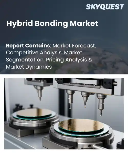
Hybrid bonding is an advanced wafer level interconnect process that joins copper pads and dielectric layers to produce ultra dense resistance connections between stacked dies. Its primary driver is surging demand for bandwidth and energy efficiency as workloads in artificial intelligence, high performance computing and 5G push limits and require integration. The market evolved from through silicon vias and micro bump assembly as planarization and alignment technologies improved, enabling sub ten micron pitches. For example, HBM stacks for GPUs and multi die SoCs in smartphones illustrate how hybrid bonding reduces package size and enables higher data rates and lower power.A central factor shaping the hybrid bonding market is maturation of fabrication and inspection equipment, enabling yield improvements and cost declines that make volume adoption feasible. As alignment, planarization and fine pitch etch capabilities improve, yields rise and throughput increases, prompting foundries and OSATs to commercialize hybrid bonded packages at lower prices. This cost shift leads OEMs to specify stacked HBM for GPUs, chiplet SoCs in smartphones and compact AI accelerators for edge servers, which creates opportunities for OSATs and design houses to monetize modular designs and for automotive and industrial manufacturers to integrate dense, low latency assemblies into products.
How is AI enhancing alignment precision in the hybrid bonding market?
AI enhances alignment precision in the hybrid bonding market by combining high resolution machine vision with deep learning models and adaptive control to correct drift and overlay variability. Systems now fuse visual inspection and inline metrology so algorithms can predict distortions and steer actuators for repeatable submicron placement. In practice this reduces scrap and shortens cycle time while enabling tighter interconnect pitches required for advanced packaging and 3D integration. Vendors and research centers are integrating these capabilities into production tools to improve yield and throughput and to meet growing demand for high performance memory and AI accelerators.EV Group May 2026, demonstrated record post bonding overlay accuracy in a wafer to wafer hybrid bonding test, showing how AI enabled inspection and control supports finer pitches and higher yield, accelerating adoption and production efficiency.
Market snapshot - (2026-2033)
Global Market Size
USD 165.0 Million
Largest Segment
Wafer-to-Wafer (W2W)
Fastest Growth
Die-to-Wafer (D2W)
Growth Rate
21.2% CAGR
To get more insights on this market click here to Request a Free Sample Report
Global hybrid bonding market is segmented by bonding type, equipment type, process flow, integration level, application, end user and region. Based on bonding type, the market is segmented into Wafer-to-Wafer (W2W), Die-to-Wafer (D2W) and Die-to-Die (D2D). Based on equipment type, the market is segmented into Wafer Bonders, Die Bonders and Alignment & Inspection Systems. Based on process flow, the market is segmented into Front-End (FEOL Integration) and Back-End (BEOL / Advanced Packaging). Based on integration level, the market is segmented into 2.5D Integration and 3D Integration. Based on application, the market is segmented into Memory (HBM, DRAM, NAND), Logic Devices, CMOS Image Sensors (CIS) and MEMS & Sensors. Based on end user, the market is segmented into Foundries, Integrated Device Manufacturers (IDMs) and OSAT (Outsourced Semiconductor Assembly & Test). Based on region, the market is segmented into North America, Europe, Asia Pacific, Latin America and Middle East & Africa.
Wafer-to-Wafer segment dominates because wafer-level pairing of entire wafers simplifies process scaling and reduces per-die handling complexity, enabling consistent planarization and uniform interconnect formation across large die counts. This homogenous approach reduces process variability, streamlines lithography and thermal budgets, and aligns with high volume memory and logic production models, driving capital equipment investment and adoption as manufacturers prioritize throughput, yield stability, and long term product roadmaps.
However, Die-to-Wafer segment is expanding fastest because it enables flexible heterogeneous assembly of tested dies onto processed wafers, reducing risk and supporting mixed node integration. Increased demand for custom stacks, sensor fusion, and memory logic pairing drives adoption, creating new service offerings and accelerating hybrid bonding use cases across advanced packaging ecosystems.
Alignment and Inspection Systems segment leads because precise submicron alignment and in-line defect detection form the backbone of reliable hybrid bonding. High resolution metrology and automated optical and electron inspection reduce bonding failures and enable ultra fine pitch interconnects, which are essential for high bandwidth memory and dense 3D stacks. Robust feedback loops improve process control and yield, making these systems indispensable across advanced packaging flows and capital investment decisions.
However, Die Bonders segment is witnessing the strongest growth because the rise in discrete die placement for heterogeneous integration and sensor packaging demands flexible, high speed placement with gentle handling. Innovations in adhesive free pick and place, thermal management during bonding, and modular tooling expand serviceable applications, enabling OSATs and IDMs to scale bespoke hybrid bonded packages quickly.
To get detailed segments analysis, Request a Free Sample Report
Asia Pacific dominance reflects a convergence of advanced manufacturing ecosystems, concentrated semiconductor capacity, and deep supply chain integration that collectively accelerate adoption of hybrid bonding. Strong local capabilities in materials, equipment, and process development enable rapid prototyping and scale up within regional clusters. Close proximity between design houses, foundries, and packaging specialists fosters iterative innovation and faster time to market for complex three dimensional integration. Regional policy support, targeted R and D collaborations, and a skilled workforce further reduce commercialization barriers. High local demand for compact high performance devices across consumer, enterprise, and industrial segments sustains investment in advanced interconnect technologies. The resulting agglomeration benefits create a reinforcing cycle of capability building and technology leadership across the Asia Pacific landscape.
Hybrid Bonding Market in Japan is driven by a dense network of equipment manufacturers, materials innovators, and research institutions that emphasize precision and reliability. Collaboration between legacy electronics firms and startups fosters incremental improvements in process controls and inspection capabilities. Domestic demand for miniaturized, high performance components from consumer electronics and industrial systems provides a stable pull for advanced packaging solutions. Japan focus on quality, materials science, and supply chain resilience positions the market to support complex integration projects and managed transitions from pilot lines to volume manufacturing.
Hybrid Bonding Market in South Korea benefits from a vertically integrated ecosystem anchored by major semiconductor manufacturers and responsive foundry networks. Strong ties between device designers and packaging operations enable rapid adoption of new interconnect approaches to meet aggressive performance and density targets. Local suppliers of process equipment and specialized materials provide timely support for process development and qualification. A culture of manufacturing agility, combined with emphasis on high bandwidth memory and system in package solutions, drives practical deployment of hybrid bonding across both domestic and export oriented product lines.
North America expansion is propelled by a blend of design leadership, specialized equipment suppliers, and concentrated investment in advanced packaging capacity. A vibrant ecosystem of fabless design companies, research universities, and precision equipment vendors facilitates novel architectures that rely on advanced interconnects. Strategic corporate and public investments target resilience in domestic supply chains and high value applications in computing, telecommunications, and defense, creating sustained demand for hybrid bonding capabilities. Collaborative pilot programs and regional innovation hubs shorten development cycles and lower integration risk. Access to specialized testing and assembly services supports commercialization pathways from prototypes to production. The combination of technological leadership and targeted infrastructure growth positions North America as a dynamic and influential market for advanced bonding technologies.
Hybrid Bonding Market in United States is characterized by strong collaboration between chip designers, advanced packaging service providers, and equipment manufacturers focused on performance centric applications. Innovation centers and university partnerships foster rapid iteration of bonding techniques and metrology. Industry emphasis on high bandwidth computing and security sensitive applications encourages investment in domestic packaging capability. The market benefits from access to specialized talent, capital for targeted scale up, and industrial ecosystems that support end to end development from concept to qualified production.
Hybrid Bonding Market in Canada is shaped by a focus on niche manufacturing, systems integration, and close links between research institutions and industry. Strengths include advanced materials research, sensor integration expertise, and collaborative initiatives that bridge design and packaging. Government and private partnerships emphasize workforce development and pilot production facilities to lower barriers to adoption. The market tends to support specialized applications where reliability and custom integration are critical, leveraging domestic engineering strengths and cross border collaboration with regional supply partners.
Europe is strengthening its role through coordinated investments in advanced packaging research, cross industry consortia, and the development of regional centers of excellence that bridge academia and manufacturing. The continental approach emphasizes standards, interoperability, and supply chain diversification to support industrial applications such as automotive, aerospace, and factory automation. Public private partnerships and cluster initiatives promote shared infrastructure and pilot lines that reduce risk for new process adoption. Emphasis on sustainability, process robustness, and high reliability drives tailored hybrid bonding solutions for stringent sectoral requirements. European efforts to cultivate skilled talent and localize critical portions of the value chain enhance competitiveness and enable deeper engagement with global supply networks.
Hybrid Bonding Market in Germany is anchored by strong industrial demand from automotive and machine building sectors that require rugged, high reliability solutions. Research institutes and industrial partners focus on qualification, process robustness, and integration with sensor and power electronics ecosystems. Emphasis on manufacturing quality and traceability supports the deployment of hybrid bonding in safety critical systems. Collaborative initiatives between engineering firms and packaging specialists enable targeted development of solutions tailored to demanding application environments.
Hybrid Bonding Market in United Kingdom benefits from a concentration of design houses, research laboratories, and test facilities that emphasize novel architectures and prototyping. Academic industry collaborations drive advances in metrology and process development, enabling rapid validation of new bonding approaches. The market supports specialized applications in communications and instrumentation where custom integration and high performance are critical. Focus on skills development and technology transfer helps bridge lab scale innovation to industrial adoption.
Hybrid Bonding Market in France is influenced by strong public research organizations and industrial players that prioritize materials innovation and system level integration. Collaborative frameworks support technology maturation and pilot production for applications in aerospace, defense, and industrial electronics. Emphasis on cross sector partnerships and standards development assists in aligning process qualification and supply chain coordination. The market tends to favor solutions that combine reliability with adaptability for complex, mission critical systems.
To know more about the market opportunities by region and country, click here to
Buy The Complete Report
Demand For Advanced Packaging
Miniaturization and Performance Needs
High Capital and Equipment Complexity
Material Compatibility and Reliability Challenges
Request Free Customization of this report to help us to meet your business objectives.
Competitive landscape in the global hybrid bonding market is shaped by equipment alliances, IP licensing and technology co development. Recent strategic moves include Applied Materials co developing die based hybrid bonding equipment with Besi and Adeia licensing hybrid bonding patents to Qorvo, driving supplier consolidation and differentiation through proprietary activation and cleaning modules. Mergers and targeted partnerships accelerate qualification for high volume customers.
Top Player’s Company Profile
Recent Developments
SkyQuest’s ABIRAW (Advanced Business Intelligence, Research & Analysis Wing) is our Business Information Services team that Collects, Collates, Correlates, and Analyses the Data collected by means of Primary Exploratory Research backed by robust Secondary Desk research. As per SkyQuest analysis, the global hybrid bonding market is being driven by surging demand for bandwidth and energy efficiency in AI, HPC and 5G applications, while maturation of fabrication and inspection equipment further accelerates adoption by improving yield and lowering costs. The market faces a significant restraint from high capital requirements and equipment complexity that slow wider implementation. The dominating region is Asia Pacific, supported by dense manufacturing ecosystems and strong supply chain integration, and the dominating segment is Wafer-to-Wafer bonding due to its throughput and yield advantages in high-volume memory and logic production. Overall, strong demand and equipment improvements underpin near-term growth.
| Report Metric | Details |
|---|---|
| Market size value in 2024 | USD 165.0 Million |
| Market size value in 2033 | USD 931.12 Million |
| Growth Rate | 21.2% |
| Base year | 2024 |
| Forecast period | (2026-2033) |
| Forecast Unit (Value) | USD Million |
| Segments covered |
|
| Regions covered | North America (US, Canada), Europe (Germany, France, United Kingdom, Italy, Spain, Rest of Europe), Asia Pacific (China, India, Japan, Rest of Asia-Pacific), Latin America (Brazil, Rest of Latin America), Middle East & Africa (South Africa, GCC Countries, Rest of MEA) |
| Companies covered |
|
| Customization scope | Free report customization with purchase. Customization includes:-
|
To get a free trial access to our platform which is a one stop solution for all your data requirements for quicker decision making. This platform allows you to compare markets, competitors who are prominent in the market, and mega trends that are influencing the dynamics in the market. Also, get access to detailed SkyQuest exclusive matrix.
Table Of Content
Executive Summary
Market overview
Parent Market Analysis
Market overview
Market size
KEY MARKET INSIGHTS
COVID IMPACT
MARKET DYNAMICS & OUTLOOK
Market Size by Region
KEY COMPANY PROFILES
Methodology
For the Hybrid Bonding Market, our research methodology involved a mixture of primary and secondary data sources. Key steps involved in the research process are listed below:
1. Information Procurement: This stage involved the procurement of Market data or related information via primary and secondary sources. The various secondary sources used included various company websites, annual reports, trade databases, and paid databases such as Hoover's, Bloomberg Business, Factiva, and Avention. Our team did 45 primary interactions Globally which included several stakeholders such as manufacturers, customers, key opinion leaders, etc. Overall, information procurement was one of the most extensive stages in our research process.
2. Information Analysis: This step involved triangulation of data through bottom-up and top-down approaches to estimate and validate the total size and future estimate of the Hybrid Bonding Market.
3. Report Formulation: The final step entailed the placement of data points in appropriate Market spaces in an attempt to deduce viable conclusions.
4. Validation & Publishing: Validation is the most important step in the process. Validation & re-validation via an intricately designed process helped us finalize data points to be used for final calculations. The final Market estimates and forecasts were then aligned and sent to our panel of industry experts for validation of data. Once the validation was done the report was sent to our Quality Assurance team to ensure adherence to style guides, consistency & design.
Analyst Support
Customization Options
With the given market data, our dedicated team of analysts can offer you the following customization options are available for the Hybrid Bonding Market:
Product Analysis: Product matrix, which offers a detailed comparison of the product portfolio of companies.
Regional Analysis: Further analysis of the Hybrid Bonding Market for additional countries.
Competitive Analysis: Detailed analysis and profiling of additional Market players & comparative analysis of competitive products.
Go to Market Strategy: Find the high-growth channels to invest your marketing efforts and increase your customer base.
Innovation Mapping: Identify racial solutions and innovation, connected to deep ecosystems of innovators, start-ups, academics, and strategic partners.
Category Intelligence: Customized intelligence that is relevant to their supply Markets will enable them to make smarter sourcing decisions and improve their category management.
Public Company Transcript Analysis: To improve the investment performance by generating new alpha and making better-informed decisions.
Social Media Listening: To analyze the conversations and trends happening not just around your brand, but around your industry as a whole, and use those insights to make better Marketing decisions.
REQUEST FOR SAMPLE
 REQUEST FREE CUSTOMIZATION


Want to customize this report? This report can be personalized according to your needs. Our analysts and industry experts will work directly with you to understand your requirements and provide you with customized data in a short amount of time. We offer $1000 worth of FREE customization at the time of purchase.
Feedback From Our Clients

 USA (+1) 351-333-4748
