Extreme Ultraviolet (EUV) Lithography Market

Extreme Ultraviolet (EUV) Lithography Market Size, Share, Growth Analysis, By Equipment(Light Source, Optics), By End User(Integrated Device Manufacturer (IDM), Foundries), By Region(Americas, Europe) - Industry Forecast 2024-2031


Report ID: UCMIG45N2065 | Region: Global | Published Date: Upcoming |
Pages: 165 | Tables: 55 | Figures: 60

Extreme Ultraviolet (EUV) Lithography Market Insights

Market Overview:

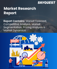
The market for EUV lithography is predicted to grow at a CAGR of 21.8% from 2023 to 2028, from USD 9.4 billion to USD 25.3 billion. The market drivers are technology that produces microchips more quickly than competing methods and chip manufacturers who streamline their production methods for greater efficiency.

Extreme Ultraviolet (EUV) Lithography Market, Forecast & Y-O-Y Growth Rate, 2020 - 2028
ForecastGrowthRate
To get more reports on the above market click here to
GET FREE SAMPLE

This report is being written to illustrate the market opportunity by region and by segments, indicating opportunity areas for the vendors to tap upon. To estimate the opportunity, it was very important to understand the current market scenario and the way it will grow in future.

Production and consumption patterns are being carefully compared to forecast the market. Other factors considered to forecast the market are the growth of the adjacent market, revenue growth of the key market vendors, scenario-based analysis, and market segment growth.

The market size was determined by estimating the market through a top-down and bottom-up approach, which was further validated with industry interviews. Considering the nature of the market we derived the Semiconductor Equipment by segment aggregation, the contribution of the Semiconductor Equipment in Semiconductors & Semiconductor Equipment and vendor share.

To determine the growth of the market factors such as drivers, trends, restraints, and opportunities were identified, and the impact of these factors was analyzed to determine the market growth. To understand the market growth in detail, we have analyzed the year-on-year growth of the market. Also, historic growth rates were compared to determine growth patterns.

Segmentation Analysis:

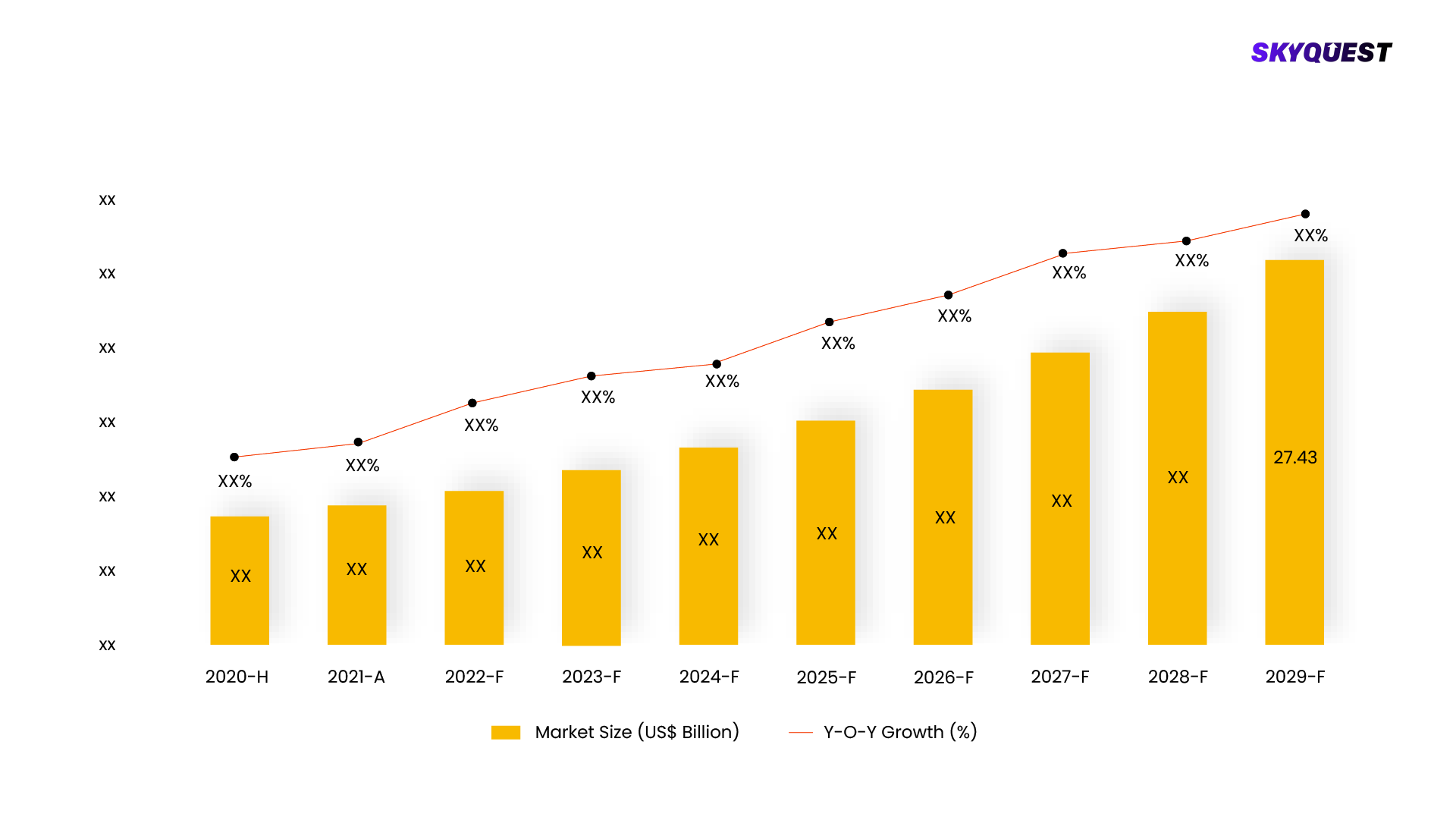
The Extreme Ultraviolet (EUV) Lithography Market is segmented by Equipment, End User, Region. We are analyzing the market of these segments to identify which segment is the largest now and in the future, which segment has the highest growth rate, and the segment which offers the opportunity in the future.

Extreme Ultraviolet (EUV) Lithography Market Basis Point Share Analysis, 2021 Vs. 2028
BasisPointShareAnalysis
To get detailed analysis on all segments
BUY NOW
  • Based on Equipment the market is segmented as, Light Source, Optics, Mask, Others
  • Based on End User the market is segmented as, Integrated Device Manufacturer (IDM), Foundries
  • Based on Region the market is segmented as, Americas, Europe, Asia Pacific, KEY MARKET PLAYERS, ASML, Carl Zeiss AG, TOPPAN Inc., NTT Advanced Technology Corporation, KLA Corporation, ADVANTEST CORPORATION, Ushio Inc., SUSS MicroTec SE, AGC Inc., Lasertec Corporation, NuFlare Technology, Energetiq Technology Inc., Photronics, Inc., HOYA Corporation, TRUMPF, Rigaku Corporation, Edmund Optics Ltd., Park Systems, Zygo Corporation, Imagine Optic, Applied Materials, Inc.

Regional Analysis:

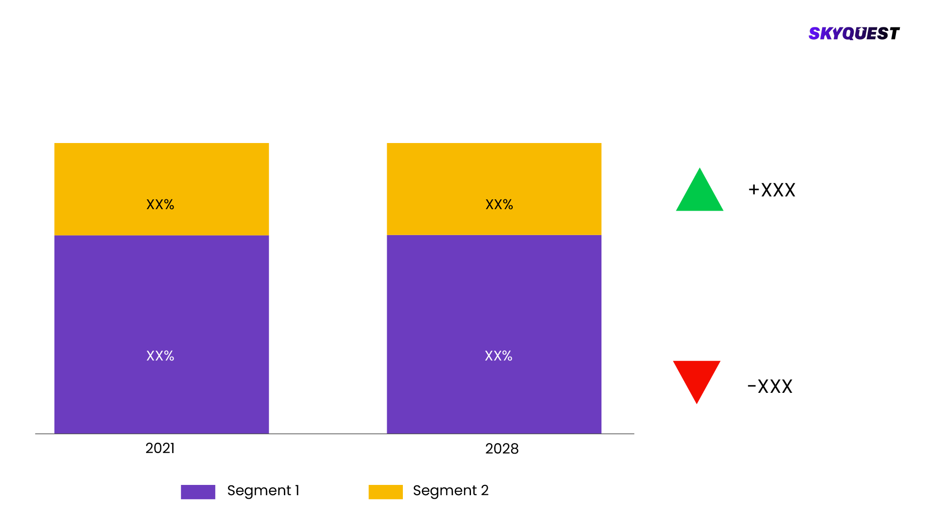
Extreme Ultraviolet (EUV) Lithography Market is being analyzed by North America, Europe, Asia-Pacific (APAC), Latin America (LATAM), Middle East & Africa (MEA) regions. Key countries including the U.S., Canada, Germany, France, UK, Italy, Spain, China, India, Japan, Brazil, GCC Countries, and South Africa among others were analyzed considering various micro and macro trends.

Extreme Ultraviolet (EUV) Lithography Market Attractiveness Analysis, By Region 2020-2028
AttractivenessAnalysis
To know more about the market opportunities by region and country, click here to
REQUEST FREE CUSTOMIZATION

Extreme Ultraviolet (EUV) Lithography Market : Risk Analysis

SkyQuest's expert analysts have conducted a risk analysis to understand the impact of external extremities on Extreme Ultraviolet (EUV) Lithography Market. We analyzed how geopolitical influence, natural disasters, climate change, legal scenario, economic impact, trade & economic policies, social & ethnic concerns, and demographic changes might affect Extreme Ultraviolet (EUV) Lithography Market's supply chain, distribution, and total revenue growth.

Competitive landscaping:

To understand the competitive landscape, we are analyzing key Extreme Ultraviolet (EUV) Lithography Market vendors in the market. To understand the competitive rivalry, we are comparing the revenue, expenses, resources, product portfolio, region coverage, market share, key initiatives, product launches, and any news related to the Extreme Ultraviolet (EUV) Lithography Market.

To validate our hypothesis and validate our findings on the market ecosystem, we are also conducting a detailed porter's five forces analysis. Competitive Rivalry, Supplier Power, Buyer Power, Threat of Substitution, and Threat of New Entry each force is analyzed by various parameters governing those forces.

Key Players Covered in the Report:

  • hography market is expected to reach USD 25.3 billion by 2028 from USD 9.4 billion in 2023, at a CAGR of 21.8% during the 2023–2028 period. Extreme Ultraviolet Lithography (EUVL) is an advanced semiconductor manufacturing technique used to create integrated circuits (ICs) with smaller feature sizes and higher precision. It is considered one of the key enabling technologies for the continued miniaturization of electronic devices. The core component of EUV lithography is a specialized light source, mask, and optics. This source generates intense pulses of EUV light by converting a high-power laser beam into EUV radiation using a process known as laser-produced plasma. The EUV light is then directed onto a mask, which contains the pattern to be printed onto the silicon wafer.
  • The EUV mask, also known as a reticle, is like traditional photomasks but has some key differences. It consists of a reflective multilayer coating on a thin silicon substrate. The reflective coating is designed to reflect EUV light while absorbing other wavelengths. The mask pattern is etched into the reflective coating, and when illuminated by EUV light, the pattern is projected onto the silicon wafer. Also, EUV optics play a vital role in shaping, focusing, and directing the intense EUV light used in the lithography process.
  • EUV Lithography
  • Driver: Increasing complexity of the integrated circuit.
  • The increasing complexity of integrated circuits (ICs) refers to the growing demand for semiconductor devices with more intricate and sophisticated designs. As ICs become more advanced, they require finer and more precise lithography techniques to achieve the desired performance and functionality. This complexity is driven by several factors, including the need for higher transistor density, smaller feature sizes, and the integration of new device architectures.
  • EUV lithography serves as a crucial driver for the market because it enables the fabrication of these complex ICs. EUV lithography technology utilizes extreme ultraviolet light with a shorter wavelength to print smaller and more intricate patterns on semiconductor wafers. With its superior resolution and better control over critical dimensions, EUV lithography allows semiconductor manufacturers to achieve the required precision and accuracy for advanced IC designs.
  • As the complexity of ICs increases, traditional lithography techniques face limitations in terms of resolution and pattern fidelity. EUV lithography overcomes these limitations, providing the capability to print smaller features and tighter patterns. This is particularly important for manufacturing high-performance chips used in applications such as artificial intelligence, 5G connectivity, data centers, and autonomous vehicles.
  • Restraint: High cost of implementing EUV Lithography system.
  • The high cost associated with implementing EUV lithography is a significant restraining factor. The technology requires the development of expensive and complex equipment, including EUV light sources, masks, and photoresists. The current cost of EUV lithography machines is several times higher than traditional optical lithography tools. This cost factor presents a barrier for smaller semiconductor manufacturers or foundries that may not have the financial resources to adopt EUV lithography technology. EUV lithography requires specialized and complex equipment, which significantly contributes to the high implementation cost. Key components include EUV light sources, masks (reticles), photoresists, and scanners. These components are expensive to develop, manufacture, and maintain. In comparison with masks used in traditional optical lithography, EUV masks are more intricate and expensive to produce.
  • Opportunity: Advanced memory development for next-generation memory devices.
  • The expansion of EUV (Extreme Ultraviolet) lithography in memory manufacturing presents a significant opportunity for the EUV lithography market. Memory devices, such as DRAM (Dynamic Random Access Memory) and NAND Flash, play a crucial role in various electronic devices, including computers, smartphones, and data centers. As memory technology advances, there is a growing demand for higher capacity, faster, and more energy-efficient memory solutions. EUV lithography offers unique advantages that make it an attractive option for the production of advanced memory devices.
  • EUV lithography's ability to deliver high-resolution imaging and precise patterning enables the creation of smaller and denser memory cells. This is particularly important in the context of next-generation memory technologies, such as EUV-based DRAM and 3D NAND Flash. By using EUV lithography, memory manufacturers can overcome the limitations of traditional optical lithography, which struggles to achieve the necessary resolution and pattern fidelity for advanced memory designs.
  • One of the main advantages of EUV lithography in memory manufacturing is its ability to pattern complex three-dimensional structures. EUV lithography can contribute to the development of advanced DRAM technologies, such as EUV-based High Bandwidth Memory (HBM). HBM offers significantly higher bandwidth and improved power efficiency compared to traditional memory solutions. By utilizing EUV lithography, memory manufacturers can fabricate the intricate interconnects and through-silicon vias (TSVs) required in HBM, enabling higher memory bandwidth and improved performance in applications like graphics processing units (GPUs) and artificial intelligence (AI) accelerators.
  • Challenge: Source power and productivity in EUV lithography act as a challenge for the market
  • Source power and productivity are significant challenges in the EUV (Extreme Ultraviolet) lithography market. The source power refers to the intensity of the EUV light generated by the light source used in the lithography system. It directly influences the speed and efficiency of the lithography process, while productivity refers to the overall throughput and capacity of the system to process wafers.
  • The availability of high-source power is crucial for achieving faster exposure times and higher wafer throughput, which are essential for meeting the demands of high-volume semiconductor manufacturing. Higher source power allows for more efficient exposure, reducing the time it takes to expose each individual wafer and increasing the number of wafers processed per unit of time.
  • Achieving and maintaining high source power in EUV lithography systems is a significant technical challenge. Generating stable and reliable EUV light at the required power levels is complex and requires advanced technologies. Additionally, maintaining the source power over extended periods of operation without degradation is a continuous challenge.
  • EUV Lithography Market Ecosystem
  • The prominent players in the EUV lithography market are ASML (Netherlands), Carl Zeiss AG(Germany), TOPPAN Inc. (Japan), HOYA Corporation (Japan), TRUMPF (Germany), and KLA Corporation (US). These companies not only boast a comprehensive product portfolio of EUV lithography but also have a strong geographic footprint.
  • The EUV light source holds the largest market share of the equipment segment in the EUV lithography market during the forecast period
  • The EUV Lithography light source is a crucial component used in the semiconductor industry's EUV lithography systems. Currently, the primary method for generating EUV light is through laser-produced plasma (LPP) technology. ASML, a prominent semiconductor equipment manufacturer, has developed a notable LPP EUV light source. This particular light source utilizes a high-power pulsed laser to irradiate tin (Sn) droplets or a thin tin film. The laser's energy causes rapid heating and vaporization of the tin material, creating plasma. As the plasma cools and recombines, it emits EUV light with a wavelength of approximately 13.5 nanometers. ASML, Ushio Inc., Energetiq Technology Inc., and TRUMPF are among the companies providing EUV lithography light sources.
  • Foundry holds the largest market share of the EUV lithography market in 2023
  • A foundry is a specialized manufacturing facility that offers semiconductor fabrication services to semiconductor companies or integrated device manufacturers (IDMs). Foundries focus exclusively on the manufacturing aspect of the semiconductor industry and do not involve themselves in chip design. The role of foundries in the semiconductor industry is crucial as they provide manufacturing services to companies that lack their own fabrication facilities or choose to outsource their chip production. Fabless companies and IDMs collaborate with foundries to transfer their chip designs, known as intellectual property (IP), to the foundry for fabrication. Well-known foundries that provide semiconductor manufacturing services, including EUV lithography, include Taiwan Semiconductor Manufacturing Company Limited, GlobalFoundries, Samsung Foundry, and others.
  • Asia Pacific is expected to register the highest market share during the forecast period.
  • The Asia Pacific region holds immense significance in the field of EUV (Extreme Ultraviolet) lithography, an advanced technology used in semiconductor manufacturing. When analyzing the EUV lithography market in this region, countries such as China, Japan, Taiwan, South Korea, and the rest of Asia Pacific are taken into consideration. These nations have made substantial investments in the development and implementation of EUV lithography technology. They have established state-of-the-art semiconductor fabrication facilities and research institutes that focus on advancing the capabilities of EUV lithography. The strong presence of these countries in the semiconductor industry creates a high demand for EUV lithography, thereby driving its ongoing development and optimization.
  • Moreover, the Asia Pacific region boasts a large consumer electronics market, encompassing smartphones, tablets, and various electronic devices. The growing need for smaller, faster, and more energy-efficient semiconductors is propelling the adoption of advanced lithography technologies like EUV. EUV lithography enables the production of high-density and high-performance chips, which are essential for meeting the demands of the consumer electronics market in the Asia Pacific region. Additionally, this region serves as a major hub for semiconductor equipment manufacturing companies such as TOPPAN Inc., NTT Advanced Technology Corporation, ADVANTEST CORPORATION, Ushio Inc., AGC Inc., Lasertec Corporation, and NuFlare Technology etc.
  • Recent Developments
  • In January 2022, ASML announced the last phase of collaboration with Intel Corporation to drive High- NA into manufacturing in 2025. The main objective is to advance the cutting edge of semiconductor lithography technology. The first purchase order issued by Intel Corporation to ASML for the delivery of the industry’s first TWINSCAN EXE:5200 system – an extreme ultraviolet (EUV) high-volume production system with a more than 200 wafers per hour productivity and huge numerical aperture and – as part of their long-term High-NA collaboration framework.
  • In December 2022, Carl Zeiss AG developed a dedicated optical system exclusively for EUV lithography, which functions within a vacuum environment and exclusively employs mirrors. This entire system stands at approximately one and a half meters tall, weighs around 3.5 tons, and encompasses over 35,000 individual components.
  • KEY MARKET SEGMENTS
  • By Equipment
  • Light Source
  • Optics
  • Mask
  • Others
  • By End User
  • Integrated Device Manufacturer (IDM)
  • Foundries
  • By Region
  • Americas
  • Europe
  • Asia Pacific
  • KEY MARKET PLAYERS
  • ASML
  • Carl Zeiss AG
  • TOPPAN Inc.
  • NTT Advanced Technology Corporation
  • KLA Corporation
  • ADVANTEST CORPORATION
  • Ushio Inc.
  • SUSS MicroTec SE
  • AGC Inc.
  • Lasertec Corporation
  • NuFlare Technology
  • Energetiq Technology Inc.
  • Photronics, Inc.
  • HOYA Corporation
  • TRUMPF
  • Rigaku Corporation
  • Edmund Optics Ltd.
  • Park Systems
  • Zygo Corporation
  • Imagine Optic
  • Applied Materials, Inc.

SkyQuest's Expertise:

The Extreme Ultraviolet (EUV) Lithography Market is being analyzed by SkyQuest's analysts with the help of 20+ scheduled Primary interviews from both the demand and supply sides. We have already invested more than 250 hours on this report and are still refining our date to provide authenticated data to your readers and clients. Exhaustive primary and secondary research is conducted to collect information on the market, peer market, and parent market.

Our cross-industry experts and revenue-impact consultants at SkyQuest enable our clients to convert market intelligence into actionable, quantifiable results through personalized engagement.

Scope Of Report

Report Attribute Details
The base year for estimation 2021
Historical data 2016 – 2022
Forecast period 2022 – 2028
Report coverage Revenue forecast, volume forecast, company ranking, competitive landscape, growth factors, and trends, Pricing Analysis
Segments covered
  • By Equipment - Light Source, Optics, Mask, Others
  • By End User - Integrated Device Manufacturer (IDM), Foundries
  • By Region - Americas, Europe, Asia Pacific, KEY MARKET PLAYERS, ASML, Carl Zeiss AG, TOPPAN Inc., NTT Advanced Technology Corporation, KLA Corporation, ADVANTEST CORPORATION, Ushio Inc., SUSS MicroTec SE, AGC Inc., Lasertec Corporation, NuFlare Technology, Energetiq Technology Inc., Photronics, Inc., HOYA Corporation, TRUMPF, Rigaku Corporation, Edmund Optics Ltd., Park Systems, Zygo Corporation, Imagine Optic, Applied Materials, Inc.
Regional scope North America, Europe, Asia-Pacific (APAC), Latin America (LATAM), Middle East & Africa (MEA)
Country scope U.S., Canada, Germany, France, UK, Italy, Spain, China, India, Japan, Brazil, GCC Countries, South Africa
Key companies profiled
  • hography market is expected to reach USD 25.3 billion by 2028 from USD 9.4 billion in 2023, at a CAGR of 21.8% during the 2023–2028 period. Extreme Ultraviolet Lithography (EUVL) is an advanced semiconductor manufacturing technique used to create integrated circuits (ICs) with smaller feature sizes and higher precision. It is considered one of the key enabling technologies for the continued miniaturization of electronic devices. The core component of EUV lithography is a specialized light source, mask, and optics. This source generates intense pulses of EUV light by converting a high-power laser beam into EUV radiation using a process known as laser-produced plasma. The EUV light is then directed onto a mask, which contains the pattern to be printed onto the silicon wafer.
  • The EUV mask, also known as a reticle, is like traditional photomasks but has some key differences. It consists of a reflective multilayer coating on a thin silicon substrate. The reflective coating is designed to reflect EUV light while absorbing other wavelengths. The mask pattern is etched into the reflective coating, and when illuminated by EUV light, the pattern is projected onto the silicon wafer. Also, EUV optics play a vital role in shaping, focusing, and directing the intense EUV light used in the lithography process.
  • EUV Lithography
  • Driver: Increasing complexity of the integrated circuit.
  • The increasing complexity of integrated circuits (ICs) refers to the growing demand for semiconductor devices with more intricate and sophisticated designs. As ICs become more advanced, they require finer and more precise lithography techniques to achieve the desired performance and functionality. This complexity is driven by several factors, including the need for higher transistor density, smaller feature sizes, and the integration of new device architectures.
  • EUV lithography serves as a crucial driver for the market because it enables the fabrication of these complex ICs. EUV lithography technology utilizes extreme ultraviolet light with a shorter wavelength to print smaller and more intricate patterns on semiconductor wafers. With its superior resolution and better control over critical dimensions, EUV lithography allows semiconductor manufacturers to achieve the required precision and accuracy for advanced IC designs.
  • As the complexity of ICs increases, traditional lithography techniques face limitations in terms of resolution and pattern fidelity. EUV lithography overcomes these limitations, providing the capability to print smaller features and tighter patterns. This is particularly important for manufacturing high-performance chips used in applications such as artificial intelligence, 5G connectivity, data centers, and autonomous vehicles.
  • Restraint: High cost of implementing EUV Lithography system.
  • The high cost associated with implementing EUV lithography is a significant restraining factor. The technology requires the development of expensive and complex equipment, including EUV light sources, masks, and photoresists. The current cost of EUV lithography machines is several times higher than traditional optical lithography tools. This cost factor presents a barrier for smaller semiconductor manufacturers or foundries that may not have the financial resources to adopt EUV lithography technology. EUV lithography requires specialized and complex equipment, which significantly contributes to the high implementation cost. Key components include EUV light sources, masks (reticles), photoresists, and scanners. These components are expensive to develop, manufacture, and maintain. In comparison with masks used in traditional optical lithography, EUV masks are more intricate and expensive to produce.
  • Opportunity: Advanced memory development for next-generation memory devices.
  • The expansion of EUV (Extreme Ultraviolet) lithography in memory manufacturing presents a significant opportunity for the EUV lithography market. Memory devices, such as DRAM (Dynamic Random Access Memory) and NAND Flash, play a crucial role in various electronic devices, including computers, smartphones, and data centers. As memory technology advances, there is a growing demand for higher capacity, faster, and more energy-efficient memory solutions. EUV lithography offers unique advantages that make it an attractive option for the production of advanced memory devices.
  • EUV lithography's ability to deliver high-resolution imaging and precise patterning enables the creation of smaller and denser memory cells. This is particularly important in the context of next-generation memory technologies, such as EUV-based DRAM and 3D NAND Flash. By using EUV lithography, memory manufacturers can overcome the limitations of traditional optical lithography, which struggles to achieve the necessary resolution and pattern fidelity for advanced memory designs.
  • One of the main advantages of EUV lithography in memory manufacturing is its ability to pattern complex three-dimensional structures. EUV lithography can contribute to the development of advanced DRAM technologies, such as EUV-based High Bandwidth Memory (HBM). HBM offers significantly higher bandwidth and improved power efficiency compared to traditional memory solutions. By utilizing EUV lithography, memory manufacturers can fabricate the intricate interconnects and through-silicon vias (TSVs) required in HBM, enabling higher memory bandwidth and improved performance in applications like graphics processing units (GPUs) and artificial intelligence (AI) accelerators.
  • Challenge: Source power and productivity in EUV lithography act as a challenge for the market
  • Source power and productivity are significant challenges in the EUV (Extreme Ultraviolet) lithography market. The source power refers to the intensity of the EUV light generated by the light source used in the lithography system. It directly influences the speed and efficiency of the lithography process, while productivity refers to the overall throughput and capacity of the system to process wafers.
  • The availability of high-source power is crucial for achieving faster exposure times and higher wafer throughput, which are essential for meeting the demands of high-volume semiconductor manufacturing. Higher source power allows for more efficient exposure, reducing the time it takes to expose each individual wafer and increasing the number of wafers processed per unit of time.
  • Achieving and maintaining high source power in EUV lithography systems is a significant technical challenge. Generating stable and reliable EUV light at the required power levels is complex and requires advanced technologies. Additionally, maintaining the source power over extended periods of operation without degradation is a continuous challenge.
  • EUV Lithography Market Ecosystem
  • The prominent players in the EUV lithography market are ASML (Netherlands), Carl Zeiss AG(Germany), TOPPAN Inc. (Japan), HOYA Corporation (Japan), TRUMPF (Germany), and KLA Corporation (US). These companies not only boast a comprehensive product portfolio of EUV lithography but also have a strong geographic footprint.
  • The EUV light source holds the largest market share of the equipment segment in the EUV lithography market during the forecast period
  • The EUV Lithography light source is a crucial component used in the semiconductor industry's EUV lithography systems. Currently, the primary method for generating EUV light is through laser-produced plasma (LPP) technology. ASML, a prominent semiconductor equipment manufacturer, has developed a notable LPP EUV light source. This particular light source utilizes a high-power pulsed laser to irradiate tin (Sn) droplets or a thin tin film. The laser's energy causes rapid heating and vaporization of the tin material, creating plasma. As the plasma cools and recombines, it emits EUV light with a wavelength of approximately 13.5 nanometers. ASML, Ushio Inc., Energetiq Technology Inc., and TRUMPF are among the companies providing EUV lithography light sources.
  • Foundry holds the largest market share of the EUV lithography market in 2023
  • A foundry is a specialized manufacturing facility that offers semiconductor fabrication services to semiconductor companies or integrated device manufacturers (IDMs). Foundries focus exclusively on the manufacturing aspect of the semiconductor industry and do not involve themselves in chip design. The role of foundries in the semiconductor industry is crucial as they provide manufacturing services to companies that lack their own fabrication facilities or choose to outsource their chip production. Fabless companies and IDMs collaborate with foundries to transfer their chip designs, known as intellectual property (IP), to the foundry for fabrication. Well-known foundries that provide semiconductor manufacturing services, including EUV lithography, include Taiwan Semiconductor Manufacturing Company Limited, GlobalFoundries, Samsung Foundry, and others.
  • Asia Pacific is expected to register the highest market share during the forecast period.
  • The Asia Pacific region holds immense significance in the field of EUV (Extreme Ultraviolet) lithography, an advanced technology used in semiconductor manufacturing. When analyzing the EUV lithography market in this region, countries such as China, Japan, Taiwan, South Korea, and the rest of Asia Pacific are taken into consideration. These nations have made substantial investments in the development and implementation of EUV lithography technology. They have established state-of-the-art semiconductor fabrication facilities and research institutes that focus on advancing the capabilities of EUV lithography. The strong presence of these countries in the semiconductor industry creates a high demand for EUV lithography, thereby driving its ongoing development and optimization.
  • Moreover, the Asia Pacific region boasts a large consumer electronics market, encompassing smartphones, tablets, and various electronic devices. The growing need for smaller, faster, and more energy-efficient semiconductors is propelling the adoption of advanced lithography technologies like EUV. EUV lithography enables the production of high-density and high-performance chips, which are essential for meeting the demands of the consumer electronics market in the Asia Pacific region. Additionally, this region serves as a major hub for semiconductor equipment manufacturing companies such as TOPPAN Inc., NTT Advanced Technology Corporation, ADVANTEST CORPORATION, Ushio Inc., AGC Inc., Lasertec Corporation, and NuFlare Technology etc.
  • Recent Developments
  • In January 2022, ASML announced the last phase of collaboration with Intel Corporation to drive High- NA into manufacturing in 2025. The main objective is to advance the cutting edge of semiconductor lithography technology. The first purchase order issued by Intel Corporation to ASML for the delivery of the industry’s first TWINSCAN EXE:5200 system – an extreme ultraviolet (EUV) high-volume production system with a more than 200 wafers per hour productivity and huge numerical aperture and – as part of their long-term High-NA collaboration framework.
  • In December 2022, Carl Zeiss AG developed a dedicated optical system exclusively for EUV lithography, which functions within a vacuum environment and exclusively employs mirrors. This entire system stands at approximately one and a half meters tall, weighs around 3.5 tons, and encompasses over 35,000 individual components.
  • KEY MARKET SEGMENTS
  • By Equipment
  • Light Source
  • Optics
  • Mask
  • Others
  • By End User
  • Integrated Device Manufacturer (IDM)
  • Foundries
  • By Region
  • Americas
  • Europe
  • Asia Pacific
  • KEY MARKET PLAYERS
  • ASML
  • Carl Zeiss AG
  • TOPPAN Inc.
  • NTT Advanced Technology Corporation
  • KLA Corporation
  • ADVANTEST CORPORATION
  • Ushio Inc.
  • SUSS MicroTec SE
  • AGC Inc.
  • Lasertec Corporation
  • NuFlare Technology
  • Energetiq Technology Inc.
  • Photronics, Inc.
  • HOYA Corporation
  • TRUMPF
  • Rigaku Corporation
  • Edmund Optics Ltd.
  • Park Systems
  • Zygo Corporation
  • Imagine Optic
  • Applied Materials, Inc.
Customization scope Free report customization (15% Free customization) with purchase. Addition or alteration to country, regional & segment scope.
Pricing and purchase options Reap the benefits of customized purchase options to fit your specific research requirements.

Objectives of the Study

  • To forecast the market size, in terms of value, for various segments with respect to five main regions, namely, North America, Europe, Asia-Pacific (APAC), Latin America (LATAM), Middle East & Africa (MEA)
  • To provide detailed information regarding the major factors influencing the growth of the Market (drivers, restraints, opportunities, and challenges)
  • To strategically analyze the micro markets with respect to the individual growth trends, future prospects, and contribution to the total market
  • To provide a detailed overview of the value chain and analyze market trends with the Porter's five forces analysis
  • To analyze the opportunities in the market for various stakeholders by identifying the high-growth Segments
  • To identify the key players and comprehensively analyze their market position in terms of ranking and core competencies, along with detailing the competitive landscape for the market leaders
  • To analyze competitive development such as joint ventures, mergers and acquisitions, new product launches and development, and research and development in the market

What does this Report Deliver?

  • Market Estimation for 20+ Countries
  • Historical data coverage: 2016 to 2022
  • Growth projections: 2022 to 2028
  • SkyQuest's premium market insights: Innovation matrix, IP analysis, Production Analysis, Value chain analysis, Technological trends, and Trade analysis
  • Customization on Segments, Regions, and Company Profiles
  • 100+ tables, 150+ Figures, 10+ matrix
  • Global and Country Market Trends
  • Comprehensive Mapping of Industry Parameters
  • Attractive Investment Proposition
  • Competitive Strategies Adopted by Leading Market Participants
  • Market drivers, restraints, opportunities, and its impact on the market
  • Regulatory scenario, regional dynamics, and insights of leading countries in each region
  • Segment trends analysis, opportunity, and growth
  • Opportunity analysis by region and country
  • Porter's five force analysis to know the market's condition
  • Pricing analysis
  • Parent market analysis
  • Product portfolio benchmarking

Table Of Content

Executive Summary

Market overview

  • Exhibit: Executive Summary – Chart on Market Overview
  • Exhibit: Executive Summary – Data Table on Market Overview
  • Exhibit: Executive Summary – Chart on Extreme Ultraviolet (EUV) Lithography Market Characteristics
  • Exhibit: Executive Summary – Chart on Market by Geography
  • Exhibit: Executive Summary – Chart on Market Segmentation
  • Exhibit: Executive Summary – Chart on Incremental Growth
  • Exhibit: Executive Summary – Data Table on Incremental Growth
  • Exhibit: Executive Summary – Chart on Vendor Market Positioning

Parent Market Analysis

Market overview

Market size

  • Market Dynamics
    • Exhibit: Impact analysis of DROC, 2021
      • Drivers
      • Opportunities
      • Restraints
      • Challenges
  • SWOT Analysis

KEY MARKET INSIGHTS

  • Technology Analysis
    • (Exhibit: Data Table: Name of technology and details)
  • Pricing Analysis
    • (Exhibit: Data Table: Name of technology and pricing details)
  • Supply Chain Analysis
    • (Exhibit: Detailed Supply Chain Presentation)
  • Value Chain Analysis
    • (Exhibit: Detailed Value Chain Presentation)
  • Ecosystem Of the Market
    • Exhibit: Parent Market Ecosystem Market Analysis
    • Exhibit: Market Characteristics of Parent Market
  • IP Analysis
    • (Exhibit: Data Table: Name of product/technology, patents filed, inventor/company name, acquiring firm)
  • Trade Analysis
    • (Exhibit: Data Table: Import and Export data details)
  • Startup Analysis
    • (Exhibit: Data Table: Emerging startups details)
  • Raw Material Analysis
    • (Exhibit: Data Table: Mapping of key raw materials)
  • Innovation Matrix
    • (Exhibit: Positioning Matrix: Mapping of new and existing technologies)
  • Pipeline product Analysis
    • (Exhibit: Data Table: Name of companies and pipeline products, regional mapping)
  • Macroeconomic Indicators

COVID IMPACT

  • Introduction
  • Impact On Economy—scenario Assessment
    • Exhibit: Data on GDP - Year-over-year growth 2016-2022 (%)
  • Revised Market Size
    • Exhibit: Data Table on Extreme Ultraviolet (EUV) Lithography Market size and forecast 2021-2027 ($ million)
  • Impact Of COVID On Key Segments
    • Exhibit: Data Table on Segment Market size and forecast 2021-2027 ($ million)
  • COVID Strategies By Company
    • Exhibit: Analysis on key strategies adopted by companies

MARKET DYNAMICS & OUTLOOK

  • Market Dynamics
    • Exhibit: Impact analysis of DROC, 2021
      • Drivers
      • Opportunities
      • Restraints
      • Challenges
  • Regulatory Landscape
    • Exhibit: Data Table on regulation from different region
  • SWOT Analysis
  • Porters Analysis
    • Competitive rivalry
      • Exhibit: Competitive rivalry Impact of key factors, 2021
    • Threat of substitute products
      • Exhibit: Threat of Substitute Products Impact of key factors, 2021
    • Bargaining power of buyers
      • Exhibit: buyers bargaining power Impact of key factors, 2021
    • Threat of new entrants
      • Exhibit: Threat of new entrants Impact of key factors, 2021
    • Bargaining power of suppliers
      • Exhibit: Threat of suppliers bargaining power Impact of key factors, 2021
  • Skyquest special insights on future disruptions
    • Political Impact
    • Economic impact
    • Social Impact
    • Technical Impact
    • Environmental Impact
    • Legal Impact

Market Size by Region

  • Chart on Market share by geography 2021-2027 (%)
  • Data Table on Market share by geography 2021-2027(%)
  • North America
    • Chart on Market share by country 2021-2027 (%)
    • Data Table on Market share by country 2021-2027(%)
    • USA
      • Exhibit: Chart on Market share 2021-2027 (%)
      • Exhibit: Market size and forecast 2021-2027 ($ million)
    • Canada
      • Exhibit: Chart on Market share 2021-2027 (%)
      • Exhibit: Market size and forecast 2021-2027 ($ million)
  • Europe
    • Chart on Market share by country 2021-2027 (%)
    • Data Table on Market share by country 2021-2027(%)
    • Germany
      • Exhibit: Chart on Market share 2021-2027 (%)
      • Exhibit: Market size and forecast 2021-2027 ($ million)
    • Spain
      • Exhibit: Chart on Market share 2021-2027 (%)
      • Exhibit: Market size and forecast 2021-2027 ($ million)
    • France
      • Exhibit: Chart on Market share 2021-2027 (%)
      • Exhibit: Market size and forecast 2021-2027 ($ million)
    • UK
      • Exhibit: Chart on Market share 2021-2027 (%)
      • Exhibit: Market size and forecast 2021-2027 ($ million)
    • Rest of Europe
      • Exhibit: Chart on Market share 2021-2027 (%)
      • Exhibit: Market size and forecast 2021-2027 ($ million)
  • Asia Pacific
    • Chart on Market share by country 2021-2027 (%)
    • Data Table on Market share by country 2021-2027(%)
    • China
      • Exhibit: Chart on Market share 2021-2027 (%)
      • Exhibit: Market size and forecast 2021-2027 ($ million)
    • India
      • Exhibit: Chart on Market share 2021-2027 (%)
      • Exhibit: Market size and forecast 2021-2027 ($ million)
    • Japan
      • Exhibit: Chart on Market share 2021-2027 (%)
      • Exhibit: Market size and forecast 2021-2027 ($ million)
    • South Korea
      • Exhibit: Chart on Market share 2021-2027 (%)
      • Exhibit: Market size and forecast 2021-2027 ($ million)
    • Rest of Asia Pacific
      • Exhibit: Chart on Market share 2021-2027 (%)
      • Exhibit: Market size and forecast 2021-2027 ($ million)
  • Latin America
    • Chart on Market share by country 2021-2027 (%)
    • Data Table on Market share by country 2021-2027(%)
    • Brazil
      • Exhibit: Chart on Market share 2021-2027 (%)
      • Exhibit: Market size and forecast 2021-2027 ($ million)
    • Rest of South America
      • Exhibit: Chart on Market share 2021-2027 (%)
      • Exhibit: Market size and forecast 2021-2027 ($ million)
  • Middle East & Africa (MEA)
    • Chart on Market share by country 2021-2027 (%)
    • Data Table on Market share by country 2021-2027(%)
    • GCC Countries
      • Exhibit: Chart on Market share 2021-2027 (%)
      • Exhibit: Market size and forecast 2021-2027 ($ million)
    • South Africa
      • Exhibit: Chart on Market share 2021-2027 (%)
      • Exhibit: Market size and forecast 2021-2027 ($ million)
    • Rest of MEA
      • Exhibit: Chart on Market share 2021-2027 (%)
      • Exhibit: Market size and forecast 2021-2027 ($ million)

KEY COMPANY PROFILES

  • Competitive Landscape
    • Total number of companies covered
      • Exhibit: companies covered in the report, 2021
    • Top companies market positioning
      • Exhibit: company positioning matrix, 2021
    • Top companies market Share
      • Exhibit: Pie chart analysis on company market share, 2021(%)
  • hography market is expected to reach USD 25.3 billion by 2028 from USD 9.4 billion in 2023, at a CAGR of 21.8% during the 2023–2028 period. Extreme Ultraviolet Lithography (EUVL) is an advanced semiconductor manufacturing technique used to create integrated circuits (ICs) with smaller feature sizes and higher precision. It is considered one of the key enabling technologies for the continued miniaturization of electronic devices. The core component of EUV lithography is a specialized light source, mask, and optics. This source generates intense pulses of EUV light by converting a high-power laser beam into EUV radiation using a process known as laser-produced plasma. The EUV light is then directed onto a mask, which contains the pattern to be printed onto the silicon wafer.
    • Exhibit Company Overview
    • Exhibit Business Segment Overview
    • Exhibit Financial Updates
    • Exhibit Key Developments
  • The EUV mask, also known as a reticle, is like traditional photomasks but has some key differences. It consists of a reflective multilayer coating on a thin silicon substrate. The reflective coating is designed to reflect EUV light while absorbing other wavelengths. The mask pattern is etched into the reflective coating, and when illuminated by EUV light, the pattern is projected onto the silicon wafer. Also, EUV optics play a vital role in shaping, focusing, and directing the intense EUV light used in the lithography process.
    • Exhibit Company Overview
    • Exhibit Business Segment Overview
    • Exhibit Financial Updates
    • Exhibit Key Developments
  • EUV Lithography
    • Exhibit Company Overview
    • Exhibit Business Segment Overview
    • Exhibit Financial Updates
    • Exhibit Key Developments
  • Driver: Increasing complexity of the integrated circuit.
    • Exhibit Company Overview
    • Exhibit Business Segment Overview
    • Exhibit Financial Updates
    • Exhibit Key Developments
  • The increasing complexity of integrated circuits (ICs) refers to the growing demand for semiconductor devices with more intricate and sophisticated designs. As ICs become more advanced, they require finer and more precise lithography techniques to achieve the desired performance and functionality. This complexity is driven by several factors, including the need for higher transistor density, smaller feature sizes, and the integration of new device architectures.
    • Exhibit Company Overview
    • Exhibit Business Segment Overview
    • Exhibit Financial Updates
    • Exhibit Key Developments
  • EUV lithography serves as a crucial driver for the market because it enables the fabrication of these complex ICs. EUV lithography technology utilizes extreme ultraviolet light with a shorter wavelength to print smaller and more intricate patterns on semiconductor wafers. With its superior resolution and better control over critical dimensions, EUV lithography allows semiconductor manufacturers to achieve the required precision and accuracy for advanced IC designs.
    • Exhibit Company Overview
    • Exhibit Business Segment Overview
    • Exhibit Financial Updates
    • Exhibit Key Developments
  • As the complexity of ICs increases, traditional lithography techniques face limitations in terms of resolution and pattern fidelity. EUV lithography overcomes these limitations, providing the capability to print smaller features and tighter patterns. This is particularly important for manufacturing high-performance chips used in applications such as artificial intelligence, 5G connectivity, data centers, and autonomous vehicles.
    • Exhibit Company Overview
    • Exhibit Business Segment Overview
    • Exhibit Financial Updates
    • Exhibit Key Developments
  • Restraint: High cost of implementing EUV Lithography system.
    • Exhibit Company Overview
    • Exhibit Business Segment Overview
    • Exhibit Financial Updates
    • Exhibit Key Developments
  • The high cost associated with implementing EUV lithography is a significant restraining factor. The technology requires the development of expensive and complex equipment, including EUV light sources, masks, and photoresists. The current cost of EUV lithography machines is several times higher than traditional optical lithography tools. This cost factor presents a barrier for smaller semiconductor manufacturers or foundries that may not have the financial resources to adopt EUV lithography technology. EUV lithography requires specialized and complex equipment, which significantly contributes to the high implementation cost. Key components include EUV light sources, masks (reticles), photoresists, and scanners. These components are expensive to develop, manufacture, and maintain. In comparison with masks used in traditional optical lithography, EUV masks are more intricate and expensive to produce.
    • Exhibit Company Overview
    • Exhibit Business Segment Overview
    • Exhibit Financial Updates
    • Exhibit Key Developments
  • Opportunity: Advanced memory development for next-generation memory devices.
    • Exhibit Company Overview
    • Exhibit Business Segment Overview
    • Exhibit Financial Updates
    • Exhibit Key Developments
  • The expansion of EUV (Extreme Ultraviolet) lithography in memory manufacturing presents a significant opportunity for the EUV lithography market. Memory devices, such as DRAM (Dynamic Random Access Memory) and NAND Flash, play a crucial role in various electronic devices, including computers, smartphones, and data centers. As memory technology advances, there is a growing demand for higher capacity, faster, and more energy-efficient memory solutions. EUV lithography offers unique advantages that make it an attractive option for the production of advanced memory devices.
    • Exhibit Company Overview
    • Exhibit Business Segment Overview
    • Exhibit Financial Updates
    • Exhibit Key Developments
  • EUV lithography's ability to deliver high-resolution imaging and precise patterning enables the creation of smaller and denser memory cells. This is particularly important in the context of next-generation memory technologies, such as EUV-based DRAM and 3D NAND Flash. By using EUV lithography, memory manufacturers can overcome the limitations of traditional optical lithography, which struggles to achieve the necessary resolution and pattern fidelity for advanced memory designs.
    • Exhibit Company Overview
    • Exhibit Business Segment Overview
    • Exhibit Financial Updates
    • Exhibit Key Developments
  • One of the main advantages of EUV lithography in memory manufacturing is its ability to pattern complex three-dimensional structures. EUV lithography can contribute to the development of advanced DRAM technologies, such as EUV-based High Bandwidth Memory (HBM). HBM offers significantly higher bandwidth and improved power efficiency compared to traditional memory solutions. By utilizing EUV lithography, memory manufacturers can fabricate the intricate interconnects and through-silicon vias (TSVs) required in HBM, enabling higher memory bandwidth and improved performance in applications like graphics processing units (GPUs) and artificial intelligence (AI) accelerators.
    • Exhibit Company Overview
    • Exhibit Business Segment Overview
    • Exhibit Financial Updates
    • Exhibit Key Developments
  • Challenge: Source power and productivity in EUV lithography act as a challenge for the market
    • Exhibit Company Overview
    • Exhibit Business Segment Overview
    • Exhibit Financial Updates
    • Exhibit Key Developments
  • Source power and productivity are significant challenges in the EUV (Extreme Ultraviolet) lithography market. The source power refers to the intensity of the EUV light generated by the light source used in the lithography system. It directly influences the speed and efficiency of the lithography process, while productivity refers to the overall throughput and capacity of the system to process wafers.
    • Exhibit Company Overview
    • Exhibit Business Segment Overview
    • Exhibit Financial Updates
    • Exhibit Key Developments
  • The availability of high-source power is crucial for achieving faster exposure times and higher wafer throughput, which are essential for meeting the demands of high-volume semiconductor manufacturing. Higher source power allows for more efficient exposure, reducing the time it takes to expose each individual wafer and increasing the number of wafers processed per unit of time.
    • Exhibit Company Overview
    • Exhibit Business Segment Overview
    • Exhibit Financial Updates
    • Exhibit Key Developments
  • Achieving and maintaining high source power in EUV lithography systems is a significant technical challenge. Generating stable and reliable EUV light at the required power levels is complex and requires advanced technologies. Additionally, maintaining the source power over extended periods of operation without degradation is a continuous challenge.
    • Exhibit Company Overview
    • Exhibit Business Segment Overview
    • Exhibit Financial Updates
    • Exhibit Key Developments
  • EUV Lithography Market Ecosystem
    • Exhibit Company Overview
    • Exhibit Business Segment Overview
    • Exhibit Financial Updates
    • Exhibit Key Developments
  • The prominent players in the EUV lithography market are ASML (Netherlands), Carl Zeiss AG(Germany), TOPPAN Inc. (Japan), HOYA Corporation (Japan), TRUMPF (Germany), and KLA Corporation (US). These companies not only boast a comprehensive product portfolio of EUV lithography but also have a strong geographic footprint.
    • Exhibit Company Overview
    • Exhibit Business Segment Overview
    • Exhibit Financial Updates
    • Exhibit Key Developments
  • The EUV light source holds the largest market share of the equipment segment in the EUV lithography market during the forecast period
    • Exhibit Company Overview
    • Exhibit Business Segment Overview
    • Exhibit Financial Updates
    • Exhibit Key Developments
  • The EUV Lithography light source is a crucial component used in the semiconductor industry's EUV lithography systems. Currently, the primary method for generating EUV light is through laser-produced plasma (LPP) technology. ASML, a prominent semiconductor equipment manufacturer, has developed a notable LPP EUV light source. This particular light source utilizes a high-power pulsed laser to irradiate tin (Sn) droplets or a thin tin film. The laser's energy causes rapid heating and vaporization of the tin material, creating plasma. As the plasma cools and recombines, it emits EUV light with a wavelength of approximately 13.5 nanometers. ASML, Ushio Inc., Energetiq Technology Inc., and TRUMPF are among the companies providing EUV lithography light sources.
    • Exhibit Company Overview
    • Exhibit Business Segment Overview
    • Exhibit Financial Updates
    • Exhibit Key Developments
  • Foundry holds the largest market share of the EUV lithography market in 2023
    • Exhibit Company Overview
    • Exhibit Business Segment Overview
    • Exhibit Financial Updates
    • Exhibit Key Developments
  • A foundry is a specialized manufacturing facility that offers semiconductor fabrication services to semiconductor companies or integrated device manufacturers (IDMs). Foundries focus exclusively on the manufacturing aspect of the semiconductor industry and do not involve themselves in chip design. The role of foundries in the semiconductor industry is crucial as they provide manufacturing services to companies that lack their own fabrication facilities or choose to outsource their chip production. Fabless companies and IDMs collaborate with foundries to transfer their chip designs, known as intellectual property (IP), to the foundry for fabrication. Well-known foundries that provide semiconductor manufacturing services, including EUV lithography, include Taiwan Semiconductor Manufacturing Company Limited, GlobalFoundries, Samsung Foundry, and others.
    • Exhibit Company Overview
    • Exhibit Business Segment Overview
    • Exhibit Financial Updates
    • Exhibit Key Developments
  • Asia Pacific is expected to register the highest market share during the forecast period.
    • Exhibit Company Overview
    • Exhibit Business Segment Overview
    • Exhibit Financial Updates
    • Exhibit Key Developments
  • The Asia Pacific region holds immense significance in the field of EUV (Extreme Ultraviolet) lithography, an advanced technology used in semiconductor manufacturing. When analyzing the EUV lithography market in this region, countries such as China, Japan, Taiwan, South Korea, and the rest of Asia Pacific are taken into consideration. These nations have made substantial investments in the development and implementation of EUV lithography technology. They have established state-of-the-art semiconductor fabrication facilities and research institutes that focus on advancing the capabilities of EUV lithography. The strong presence of these countries in the semiconductor industry creates a high demand for EUV lithography, thereby driving its ongoing development and optimization.
    • Exhibit Company Overview
    • Exhibit Business Segment Overview
    • Exhibit Financial Updates
    • Exhibit Key Developments
  • Moreover, the Asia Pacific region boasts a large consumer electronics market, encompassing smartphones, tablets, and various electronic devices. The growing need for smaller, faster, and more energy-efficient semiconductors is propelling the adoption of advanced lithography technologies like EUV. EUV lithography enables the production of high-density and high-performance chips, which are essential for meeting the demands of the consumer electronics market in the Asia Pacific region. Additionally, this region serves as a major hub for semiconductor equipment manufacturing companies such as TOPPAN Inc., NTT Advanced Technology Corporation, ADVANTEST CORPORATION, Ushio Inc., AGC Inc., Lasertec Corporation, and NuFlare Technology etc.
    • Exhibit Company Overview
    • Exhibit Business Segment Overview
    • Exhibit Financial Updates
    • Exhibit Key Developments
  • Recent Developments
    • Exhibit Company Overview
    • Exhibit Business Segment Overview
    • Exhibit Financial Updates
    • Exhibit Key Developments
  • In January 2022, ASML announced the last phase of collaboration with Intel Corporation to drive High- NA into manufacturing in 2025. The main objective is to advance the cutting edge of semiconductor lithography technology. The first purchase order issued by Intel Corporation to ASML for the delivery of the industry’s first TWINSCAN EXE:5200 system – an extreme ultraviolet (EUV) high-volume production system with a more than 200 wafers per hour productivity and huge numerical aperture and – as part of their long-term High-NA collaboration framework.
    • Exhibit Company Overview
    • Exhibit Business Segment Overview
    • Exhibit Financial Updates
    • Exhibit Key Developments
  • In December 2022, Carl Zeiss AG developed a dedicated optical system exclusively for EUV lithography, which functions within a vacuum environment and exclusively employs mirrors. This entire system stands at approximately one and a half meters tall, weighs around 3.5 tons, and encompasses over 35,000 individual components.
    • Exhibit Company Overview
    • Exhibit Business Segment Overview
    • Exhibit Financial Updates
    • Exhibit Key Developments
  • KEY MARKET SEGMENTS
    • Exhibit Company Overview
    • Exhibit Business Segment Overview
    • Exhibit Financial Updates
    • Exhibit Key Developments
  • By Equipment
    • Exhibit Company Overview
    • Exhibit Business Segment Overview
    • Exhibit Financial Updates
    • Exhibit Key Developments
  • Light Source
    • Exhibit Company Overview
    • Exhibit Business Segment Overview
    • Exhibit Financial Updates
    • Exhibit Key Developments
  • Optics
    • Exhibit Company Overview
    • Exhibit Business Segment Overview
    • Exhibit Financial Updates
    • Exhibit Key Developments
  • Mask
    • Exhibit Company Overview
    • Exhibit Business Segment Overview
    • Exhibit Financial Updates
    • Exhibit Key Developments
  • Others
    • Exhibit Company Overview
    • Exhibit Business Segment Overview
    • Exhibit Financial Updates
    • Exhibit Key Developments
  • By End User
    • Exhibit Company Overview
    • Exhibit Business Segment Overview
    • Exhibit Financial Updates
    • Exhibit Key Developments
  • Integrated Device Manufacturer (IDM)
    • Exhibit Company Overview
    • Exhibit Business Segment Overview
    • Exhibit Financial Updates
    • Exhibit Key Developments
  • Foundries
    • Exhibit Company Overview
    • Exhibit Business Segment Overview
    • Exhibit Financial Updates
    • Exhibit Key Developments
  • By Region
    • Exhibit Company Overview
    • Exhibit Business Segment Overview
    • Exhibit Financial Updates
    • Exhibit Key Developments
  • Americas
    • Exhibit Company Overview
    • Exhibit Business Segment Overview
    • Exhibit Financial Updates
    • Exhibit Key Developments
  • Europe
    • Exhibit Company Overview
    • Exhibit Business Segment Overview
    • Exhibit Financial Updates
    • Exhibit Key Developments
  • Asia Pacific
    • Exhibit Company Overview
    • Exhibit Business Segment Overview
    • Exhibit Financial Updates
    • Exhibit Key Developments
  • KEY MARKET PLAYERS
    • Exhibit Company Overview
    • Exhibit Business Segment Overview
    • Exhibit Financial Updates
    • Exhibit Key Developments
  • ASML
    • Exhibit Company Overview
    • Exhibit Business Segment Overview
    • Exhibit Financial Updates
    • Exhibit Key Developments
  • Carl Zeiss AG
    • Exhibit Company Overview
    • Exhibit Business Segment Overview
    • Exhibit Financial Updates
    • Exhibit Key Developments
  • TOPPAN Inc.
    • Exhibit Company Overview
    • Exhibit Business Segment Overview
    • Exhibit Financial Updates
    • Exhibit Key Developments
  • NTT Advanced Technology Corporation
    • Exhibit Company Overview
    • Exhibit Business Segment Overview
    • Exhibit Financial Updates
    • Exhibit Key Developments
  • KLA Corporation
    • Exhibit Company Overview
    • Exhibit Business Segment Overview
    • Exhibit Financial Updates
    • Exhibit Key Developments
  • ADVANTEST CORPORATION
    • Exhibit Company Overview
    • Exhibit Business Segment Overview
    • Exhibit Financial Updates
    • Exhibit Key Developments
  • Ushio Inc.
    • Exhibit Company Overview
    • Exhibit Business Segment Overview
    • Exhibit Financial Updates
    • Exhibit Key Developments
  • SUSS MicroTec SE
    • Exhibit Company Overview
    • Exhibit Business Segment Overview
    • Exhibit Financial Updates
    • Exhibit Key Developments
  • AGC Inc.
    • Exhibit Company Overview
    • Exhibit Business Segment Overview
    • Exhibit Financial Updates
    • Exhibit Key Developments
  • Lasertec Corporation
    • Exhibit Company Overview
    • Exhibit Business Segment Overview
    • Exhibit Financial Updates
    • Exhibit Key Developments
  • NuFlare Technology
    • Exhibit Company Overview
    • Exhibit Business Segment Overview
    • Exhibit Financial Updates
    • Exhibit Key Developments
  • Energetiq Technology Inc.
    • Exhibit Company Overview
    • Exhibit Business Segment Overview
    • Exhibit Financial Updates
    • Exhibit Key Developments
  • Photronics, Inc.
    • Exhibit Company Overview
    • Exhibit Business Segment Overview
    • Exhibit Financial Updates
    • Exhibit Key Developments
  • HOYA Corporation
    • Exhibit Company Overview
    • Exhibit Business Segment Overview
    • Exhibit Financial Updates
    • Exhibit Key Developments
  • TRUMPF
    • Exhibit Company Overview
    • Exhibit Business Segment Overview
    • Exhibit Financial Updates
    • Exhibit Key Developments
  • Rigaku Corporation
    • Exhibit Company Overview
    • Exhibit Business Segment Overview
    • Exhibit Financial Updates
    • Exhibit Key Developments
  • Edmund Optics Ltd.
    • Exhibit Company Overview
    • Exhibit Business Segment Overview
    • Exhibit Financial Updates
    • Exhibit Key Developments
  • Park Systems
    • Exhibit Company Overview
    • Exhibit Business Segment Overview
    • Exhibit Financial Updates
    • Exhibit Key Developments
  • Zygo Corporation
    • Exhibit Company Overview
    • Exhibit Business Segment Overview
    • Exhibit Financial Updates
    • Exhibit Key Developments
  • Imagine Optic
    • Exhibit Company Overview
    • Exhibit Business Segment Overview
    • Exhibit Financial Updates
    • Exhibit Key Developments
  • Applied Materials, Inc.
    • Exhibit Company Overview
    • Exhibit Business Segment Overview
    • Exhibit Financial Updates
    • Exhibit Key Developments

Methodology

For the Extreme Ultraviolet (EUV) Lithography Market, our research methodology involved a mixture of primary and secondary data sources. Key steps involved in the research process are listed below:

1. Information Procurement: This stage involved the procurement of Market data or related information via primary and secondary sources. The various secondary sources used included various company websites, annual reports, trade databases, and paid databases such as Hoover's, Bloomberg Business, Factiva, and Avention. Our team did 45 primary interactions Globally which included several stakeholders such as manufacturers, customers, key opinion leaders, etc. Overall, information procurement was one of the most extensive stages in our research process.

2. Information Analysis: This step involved triangulation of data through bottom-up and top-down approaches to estimate and validate the total size and future estimate of the Extreme Ultraviolet (EUV) Lithography Market.

3. Report Formulation: The final step entailed the placement of data points in appropriate Market spaces in an attempt to deduce viable conclusions.

4. Validation & Publishing: Validation is the most important step in the process. Validation & re-validation via an intricately designed process helped us finalize data points to be used for final calculations. The final Market estimates and forecasts were then aligned and sent to our panel of industry experts for validation of data. Once the validation was done the report was sent to our Quality Assurance team to ensure adherence to style guides, consistency & design.

Analyst Support

Customization Options

With the given market data, our dedicated team of analysts can offer you the following customization options are available for the Extreme Ultraviolet (EUV) Lithography Market:

Product Analysis: Product matrix, which offers a detailed comparison of the product portfolio of companies.

Regional Analysis: Further analysis of the Extreme Ultraviolet (EUV) Lithography Market for additional countries.

Competitive Analysis: Detailed analysis and profiling of additional Market players & comparative analysis of competitive products.

Go to Market Strategy: Find the high-growth channels to invest your marketing efforts and increase your customer base.

Innovation Mapping: Identify racial solutions and innovation, connected to deep ecosystems of innovators, start-ups, academics, and strategic partners.

Category Intelligence: Customized intelligence that is relevant to their supply Markets will enable them to make smarter sourcing decisions and improve their category management.

Public Company Transcript Analysis: To improve the investment performance by generating new alpha and making better-informed decisions.

Social Media Listening: To analyze the conversations and trends happening not just around your brand, but around your industry as a whole, and use those insights to make better Marketing decisions.

$5,300
BUY NOW GET FREE SAMPLE
Want to customize this report?

Our industry expert will work with you to provide you with customized data in a short amount of time.

REQUEST FREE CUSTOMIZATION

FAQs

The global market for Extreme Ultraviolet (EUV) Lithography was estimated to be valued at US$ XX Mn in 2021.

The global Extreme Ultraviolet (EUV) Lithography Market is estimated to grow at a CAGR of XX% by 2028.

The global Extreme Ultraviolet (EUV) Lithography Market is segmented on the basis of Equipment, End User, Region.

Based on region, the global Extreme Ultraviolet (EUV) Lithography Market is segmented into North America, Europe, Asia Pacific, Middle East & Africa and Latin America.

The key players operating in the global Extreme Ultraviolet (EUV) Lithography Market are hography market is expected to reach USD 25.3 billion by 2028 from USD 9.4 billion in 2023, at a CAGR of 21.8% during the 2023–2028 period. Extreme Ultraviolet Lithography (EUVL) is an advanced semiconductor manufacturing technique used to create integrated circuits (ICs) with smaller feature sizes and higher precision. It is considered one of the key enabling technologies for the continued miniaturization of electronic devices. The core component of EUV lithography is a specialized light source, mask, and optics. This source generates intense pulses of EUV light by converting a high-power laser beam into EUV radiation using a process known as laser-produced plasma. The EUV light is then directed onto a mask, which contains the pattern to be printed onto the silicon wafer. , The EUV mask, also known as a reticle, is like traditional photomasks but has some key differences. It consists of a reflective multilayer coating on a thin silicon substrate. The reflective coating is designed to reflect EUV light while absorbing other wavelengths. The mask pattern is etched into the reflective coating, and when illuminated by EUV light, the pattern is projected onto the silicon wafer. Also, EUV optics play a vital role in shaping, focusing, and directing the intense EUV light used in the lithography process. , EUV Lithography , Driver: Increasing complexity of the integrated circuit. , The increasing complexity of integrated circuits (ICs) refers to the growing demand for semiconductor devices with more intricate and sophisticated designs. As ICs become more advanced, they require finer and more precise lithography techniques to achieve the desired performance and functionality. This complexity is driven by several factors, including the need for higher transistor density, smaller feature sizes, and the integration of new device architectures. , EUV lithography serves as a crucial driver for the market because it enables the fabrication of these complex ICs. EUV lithography technology utilizes extreme ultraviolet light with a shorter wavelength to print smaller and more intricate patterns on semiconductor wafers. With its superior resolution and better control over critical dimensions, EUV lithography allows semiconductor manufacturers to achieve the required precision and accuracy for advanced IC designs. , As the complexity of ICs increases, traditional lithography techniques face limitations in terms of resolution and pattern fidelity. EUV lithography overcomes these limitations, providing the capability to print smaller features and tighter patterns. This is particularly important for manufacturing high-performance chips used in applications such as artificial intelligence, 5G connectivity, data centers, and autonomous vehicles. , Restraint: High cost of implementing EUV Lithography system. , The high cost associated with implementing EUV lithography is a significant restraining factor. The technology requires the development of expensive and complex equipment, including EUV light sources, masks, and photoresists. The current cost of EUV lithography machines is several times higher than traditional optical lithography tools. This cost factor presents a barrier for smaller semiconductor manufacturers or foundries that may not have the financial resources to adopt EUV lithography technology. EUV lithography requires specialized and complex equipment, which significantly contributes to the high implementation cost. Key components include EUV light sources, masks (reticles), photoresists, and scanners. These components are expensive to develop, manufacture, and maintain. In comparison with masks used in traditional optical lithography, EUV masks are more intricate and expensive to produce. , Opportunity: Advanced memory development for next-generation memory devices. , The expansion of EUV (Extreme Ultraviolet) lithography in memory manufacturing presents a significant opportunity for the EUV lithography market. Memory devices, such as DRAM (Dynamic Random Access Memory) and NAND Flash, play a crucial role in various electronic devices, including computers, smartphones, and data centers. As memory technology advances, there is a growing demand for higher capacity, faster, and more energy-efficient memory solutions. EUV lithography offers unique advantages that make it an attractive option for the production of advanced memory devices. , EUV lithography's ability to deliver high-resolution imaging and precise patterning enables the creation of smaller and denser memory cells. This is particularly important in the context of next-generation memory technologies, such as EUV-based DRAM and 3D NAND Flash. By using EUV lithography, memory manufacturers can overcome the limitations of traditional optical lithography, which struggles to achieve the necessary resolution and pattern fidelity for advanced memory designs. , One of the main advantages of EUV lithography in memory manufacturing is its ability to pattern complex three-dimensional structures. EUV lithography can contribute to the development of advanced DRAM technologies, such as EUV-based High Bandwidth Memory (HBM). HBM offers significantly higher bandwidth and improved power efficiency compared to traditional memory solutions. By utilizing EUV lithography, memory manufacturers can fabricate the intricate interconnects and through-silicon vias (TSVs) required in HBM, enabling higher memory bandwidth and improved performance in applications like graphics processing units (GPUs) and artificial intelligence (AI) accelerators. , Challenge: Source power and productivity in EUV lithography act as a challenge for the market , Source power and productivity are significant challenges in the EUV (Extreme Ultraviolet) lithography market. The source power refers to the intensity of the EUV light generated by the light source used in the lithography system. It directly influences the speed and efficiency of the lithography process, while productivity refers to the overall throughput and capacity of the system to process wafers. , The availability of high-source power is crucial for achieving faster exposure times and higher wafer throughput, which are essential for meeting the demands of high-volume semiconductor manufacturing. Higher source power allows for more efficient exposure, reducing the time it takes to expose each individual wafer and increasing the number of wafers processed per unit of time. , Achieving and maintaining high source power in EUV lithography systems is a significant technical challenge. Generating stable and reliable EUV light at the required power levels is complex and requires advanced technologies. Additionally, maintaining the source power over extended periods of operation without degradation is a continuous challenge. , EUV Lithography Market Ecosystem , The prominent players in the EUV lithography market are ASML (Netherlands), Carl Zeiss AG(Germany), TOPPAN Inc. (Japan), HOYA Corporation (Japan), TRUMPF (Germany), and KLA Corporation (US). These companies not only boast a comprehensive product portfolio of EUV lithography but also have a strong geographic footprint. , The EUV light source holds the largest market share of the equipment segment in the EUV lithography market during the forecast period , The EUV Lithography light source is a crucial component used in the semiconductor industry's EUV lithography systems. Currently, the primary method for generating EUV light is through laser-produced plasma (LPP) technology. ASML, a prominent semiconductor equipment manufacturer, has developed a notable LPP EUV light source. This particular light source utilizes a high-power pulsed laser to irradiate tin (Sn) droplets or a thin tin film. The laser's energy causes rapid heating and vaporization of the tin material, creating plasma. As the plasma cools and recombines, it emits EUV light with a wavelength of approximately 13.5 nanometers. ASML, Ushio Inc., Energetiq Technology Inc., and TRUMPF are among the companies providing EUV lithography light sources. , Foundry holds the largest market share of the EUV lithography market in 2023 , A foundry is a specialized manufacturing facility that offers semiconductor fabrication services to semiconductor companies or integrated device manufacturers (IDMs). Foundries focus exclusively on the manufacturing aspect of the semiconductor industry and do not involve themselves in chip design. The role of foundries in the semiconductor industry is crucial as they provide manufacturing services to companies that lack their own fabrication facilities or choose to outsource their chip production. Fabless companies and IDMs collaborate with foundries to transfer their chip designs, known as intellectual property (IP), to the foundry for fabrication. Well-known foundries that provide semiconductor manufacturing services, including EUV lithography, include Taiwan Semiconductor Manufacturing Company Limited, GlobalFoundries, Samsung Foundry, and others. , Asia Pacific is expected to register the highest market share during the forecast period. , The Asia Pacific region holds immense significance in the field of EUV (Extreme Ultraviolet) lithography, an advanced technology used in semiconductor manufacturing. When analyzing the EUV lithography market in this region, countries such as China, Japan, Taiwan, South Korea, and the rest of Asia Pacific are taken into consideration. These nations have made substantial investments in the development and implementation of EUV lithography technology. They have established state-of-the-art semiconductor fabrication facilities and research institutes that focus on advancing the capabilities of EUV lithography. The strong presence of these countries in the semiconductor industry creates a high demand for EUV lithography, thereby driving its ongoing development and optimization. , Moreover, the Asia Pacific region boasts a large consumer electronics market, encompassing smartphones, tablets, and various electronic devices. The growing need for smaller, faster, and more energy-efficient semiconductors is propelling the adoption of advanced lithography technologies like EUV. EUV lithography enables the production of high-density and high-performance chips, which are essential for meeting the demands of the consumer electronics market in the Asia Pacific region. Additionally, this region serves as a major hub for semiconductor equipment manufacturing companies such as TOPPAN Inc., NTT Advanced Technology Corporation, ADVANTEST CORPORATION, Ushio Inc., AGC Inc., Lasertec Corporation, and NuFlare Technology etc. , Recent Developments , In January 2022, ASML announced the last phase of collaboration with Intel Corporation to drive High- NA into manufacturing in 2025. The main objective is to advance the cutting edge of semiconductor lithography technology. The first purchase order issued by Intel Corporation to ASML for the delivery of the industry’s first TWINSCAN EXE:5200 system – an extreme ultraviolet (EUV) high-volume production system with a more than 200 wafers per hour productivity and huge numerical aperture and – as part of their long-term High-NA collaboration framework. , In December 2022, Carl Zeiss AG developed a dedicated optical system exclusively for EUV lithography, which functions within a vacuum environment and exclusively employs mirrors. This entire system stands at approximately one and a half meters tall, weighs around 3.5 tons, and encompasses over 35,000 individual components. , KEY MARKET SEGMENTS , By Equipment , Light Source , Optics , Mask , Others , By End User , Integrated Device Manufacturer (IDM) , Foundries , By Region , Americas , Europe , Asia Pacific, KEY MARKET PLAYERS , ASML , Carl Zeiss AG , TOPPAN Inc. , NTT Advanced Technology Corporation , KLA Corporation , ADVANTEST CORPORATION , Ushio Inc. , SUSS MicroTec SE , AGC Inc. , Lasertec Corporation , NuFlare Technology , Energetiq Technology Inc. , Photronics, Inc. , HOYA Corporation , TRUMPF , Rigaku Corporation , Edmund Optics Ltd. , Park Systems , Zygo Corporation , Imagine Optic , Applied Materials, Inc. .

Request Free Customization

Want to customize this report? This report can be personalized according to your needs. Our analysts and industry experts will work directly with you to understand your requirements and provide you with customized data in a short amount of time. We offer $1000 worth of FREE customization at the time of purchase.

logo-images

Feedback From Our Clients

Extreme Ultraviolet (EUV) Lithography Market

Product ID: UCMIG45N2065

$5,300
BUY NOW GET FREE SAMPLE